SLVSG41 January 2022 TPS7H4003-SEP
PRODUCTION DATA
- 1 Features
- 2 Applications
- 3 Description
- 4 Revision History
- 5 Pin Configuration and Functions
- 6 Specifications
-
7 Detailed Description
- 7.1 Overview
- 7.2 Functional Block Diagram
- 7.3
Feature Description
- 7.3.1 VIN and Power VIN Pins (VIN and PVIN)
- 7.3.2 Voltage Reference
- 7.3.3 Adjusting the Output Voltage
- 7.3.4 Safe Start-Up Into Prebiased Outputs
- 7.3.5 Error Amplifier
- 7.3.6 Enable and Adjust UVLO
- 7.3.7 Adjustable Switching Frequency and Synchronization (SYNC)
- 7.3.8 Soft-Start (SS/TR)
- 7.3.9 Power Good (PWRGD)
- 7.3.10 Sequencing
- 7.3.11 Output Overvoltage Protection (OVP)
- 7.3.12 Overcurrent Protection
- 7.3.13 Thermal Shutdown
- 7.3.14 Turn-On Behavior
- 7.3.15 Slope Compensation
- 7.3.16 Small Signal Model for Frequency Compensation
- 7.4 Device Functional Modes
-
8 Application and Implementation
- 8.1 Application Information
- 8.2
Typical Application
- 8.2.1 Design Requirements
- 8.2.2
Detailed Design Procedure
- 8.2.2.1 Operating Frequency
- 8.2.2.2 Output Inductor Selection
- 8.2.2.3 Output Capacitor Selection
- 8.2.2.4 Output Schottky Diode
- 8.2.2.5 Input Capacitor Selection
- 8.2.2.6 Soft-Start Capacitor Selection
- 8.2.2.7 Undervoltage Lockout (UVLO) Set Point
- 8.2.2.8 Output Voltage Feedback Resistor Selection
- 8.2.2.9 Compensation Component Selection
- 8.2.3 Parallel Operation
- 8.2.4 Application Curve
- 9 Power Supply Recommendations
- 10Layout
- 11Device and Documentation Support
- 12Mechanical, Packaging, and Orderable Information
7.3.7.3 Primary-Secondary Operation Mode
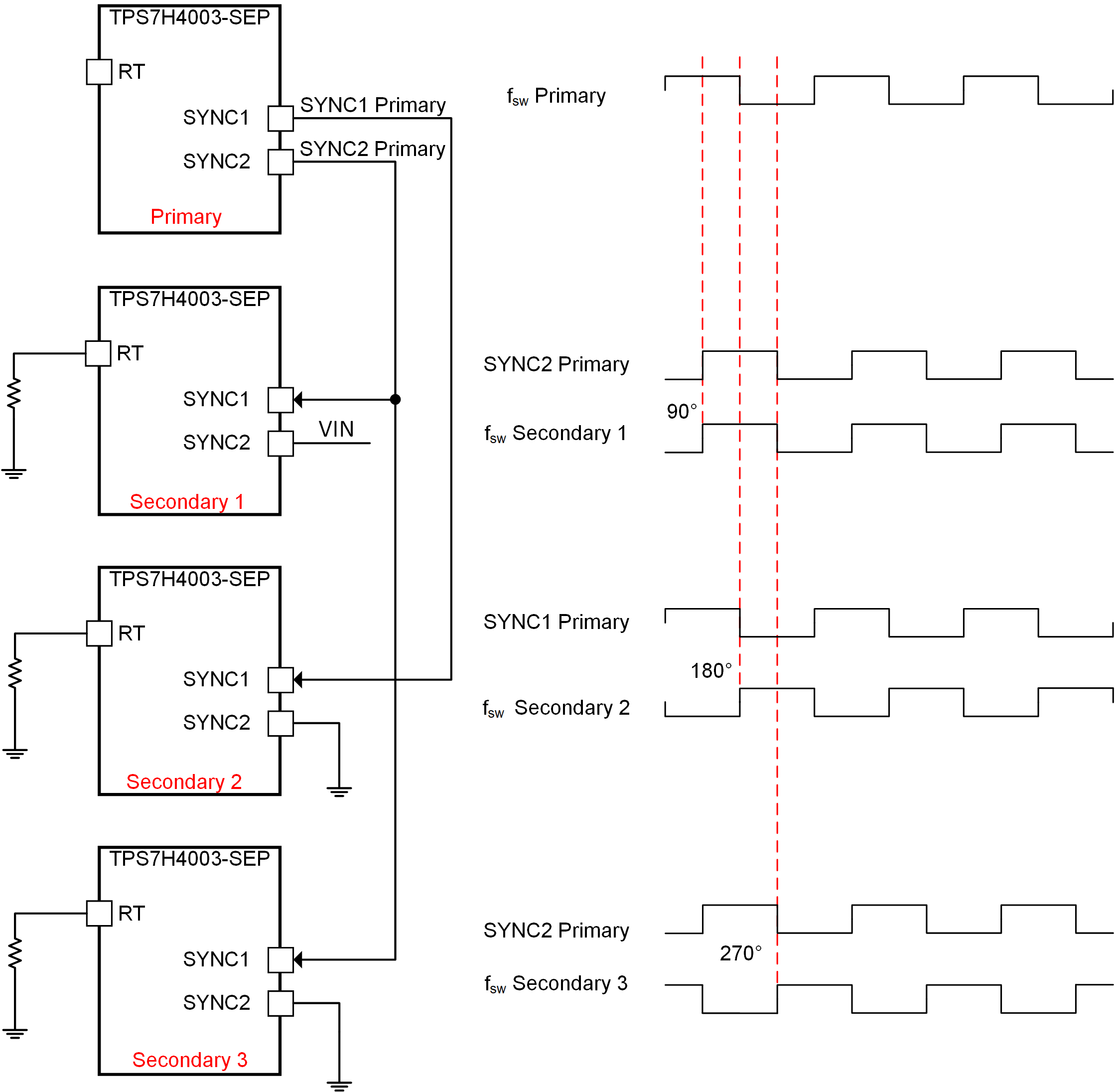
In primary-secondary mode, the RT pin of the primary device must be left floating. This sets the internal switching frequency of the device, fSW to a typical 500 kHz and the SYNC1 pin becomes an output clock at the same frequency and phase as fSW. In addition, the SYNC2 pin becomes an output clock at the same frequency but at 90° out of phase with respect to SYNC1. These SYNC1 and SYNC2 output clock signals, in combination with the state of the SYNC2 pins of the secondary devices, can be used to connect 2, 3, or 4 devices in parallel configuration. Figure 7-5 shows the SYNC1 and SYNC2 clock signals when the RT pin is floating in the primary device and how the signals can be used to generate the 90° out of phase clocks needed to connect 4 devices in parallel configuration (1 primary and 3 secondaries). The SYNC1b and SYNC2b indicate the clock signals being inverted either internally or due to the state of the SYNC2 pin in the secondary devices. When SYNC2 is connected to GND, the inverse functionality of the input clock signal in SYNC1 remains the same. When SYNC2 is connected to VIN, the input clock signal in SYNC1 does not get inverted. The RT pin of the secondary devices must have a resistor to GND corresponding to 500 kHz as indicated in Equation 4 and Figure 7-4.
 Figure 7-5 SYNC1 and SYNC2 Clock Signals
in Primary-Secondary Mode
Figure 7-5 SYNC1 and SYNC2 Clock Signals
in Primary-Secondary ModeFigure 7-6 shows the SYNC1 and SYNC2 output signals from the primary device as well as signals and connections needed to operate 4 devices in parallel configuration. The fSW clock signal by each device represents the switching frequency signal for the respective device.
 Figure 7-6 Parallel Operation With SYNC1
and SYNC2 Pins
Figure 7-6 Parallel Operation With SYNC1
and SYNC2 PinsThe 3 modes previously described are summarized in Table 7-1.
| MODE | RT PIN | SYNC1 PIN | SYNC2 PIN | SWITCHING FREQUENCY |
|---|---|---|---|---|
| Internal oscillator | Resistor to GND based on Figure 7-4 | Floating | GND | Configurable using internal oscillator from 100 kHz to 1 MHz depending on RT resistor value |
| External synchronization | External input clock. Signal will be inverted internally | GND or VIN | Internally synchronized to external clock between 100 kHz to 1 MHz | |
| Primary | Float | Outputs 500-kHz clock in phase with internal switching frequency | Outputs 500-kHz clock at 90° out of phase with internal switching frequency | 500 kHz |