SLVU097B October   2003  – October 2021 TPS54350


  1.   Trademarks
  2. 1Introduction
    1. 1.1 Background
    2. 1.2 Performance Specification Summary
    3. 1.3 Modifications
      1. 1.3.1 Output Voltage Setpoint
      2. 1.3.2 Switching Frequency
      3. 1.3.3 Input Filter
      4. 1.3.4 UVLO Programming
      5. 1.3.5 Synchronization
      6. 1.3.6 Power Good
      7. 1.3.7 Synchronous Low-Side FET
      8. 1.3.8 Optional Output Filtering
  3. 2Test Setup and Results
    1. 2.1  Input/Output Connections
    2. 2.2  Efficiency
    3. 2.3  Power Dissipation
    4. 2.4  Output Voltage Regulation
    5. 2.5  Load Transients
    6. 2.6  Loop Characteristic
    7. 2.7  Output Voltage Ripple
    8. 2.8  Input Voltage Ripple
    9. 2.9  Gate Drive
    10. 2.10 Powering Up and Down
  4. 3Board Layout
    1. 3.1 Layout
  5. 4Schematic and Bill of Materials
    1. 4.1 Bill of Materials
  6. 5Revision History

Powering Up and Down

The start-up voltage waveform of the TPS54350EVM−235 is shown in Figure 2-12. The waveform shows the nominal 12-V input voltage in Ch. 1, the 3.3-V output ramping up in Ch. 2, and the PWRGD signal in Ch. 3. Note that the PWRGD signal is pulled up externally to 3.3 V.
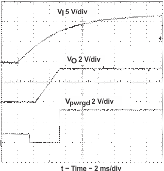
GUID-20210929-SS0I-RFVQ-QCMW-J2K2507NDSFT-low.gif Figure 2-12 Powering Up

The corresponding power-down waveform is shown in Figure 2-13. The channel assignments are the same as in the power-up waveform in Figure 2-12.
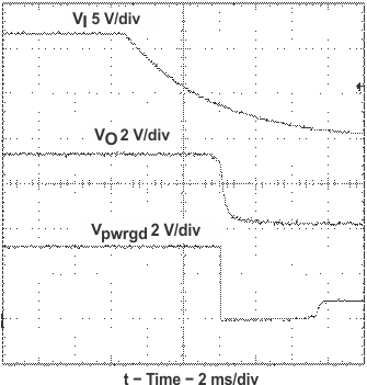
GUID-20210929-SS0I-HLD1-6LGH-N3RSXBJSDHJ5-low.gif Figure 2-13 Powering Down