SLVU793A October   2012  – June 2021 TPS56921


  1.   Trademarks
  2. 1Introduction
    1. 1.1 Background
    2. 1.2 Performance Specification Summary
    3. 1.3 Modifications
      1. 1.3.1 Output Voltage Setpoint
      2. 1.3.2 Slow-Start Time
      3. 1.3.3 Adjustable UVLO
      4. 1.3.4 Input Voltage Rails
  3. 2Test Setup and Results
    1. 2.1 Input/Output Connections
    2. 2.2 Efficiency
    3. 2.3 Output Voltage Load Regulation
    4. 2.4 Output Voltage Line Regulation
    5. 2.5 Load Transients
    6. 2.6 Loop Characteristics
    7. 2.7 Output Voltage Ripple
    8. 2.8 Input Voltage Ripple
    9. 2.9 Powering Up
  4. 3Board Layout
    1. 3.1 Layout
  5. 4Schematic and Bill of Materials
    1. 4.1 Schematic
    2. 4.2 Bill of Materials
  6. 5Revision History

Output Voltage Ripple

Figure 2-8 shows the TPS56921EVM-188 output voltage ripple. The output current is the rated full load of 9 A and VIN = 12 V. The ripple voltage is measured directly across the output capacitors.
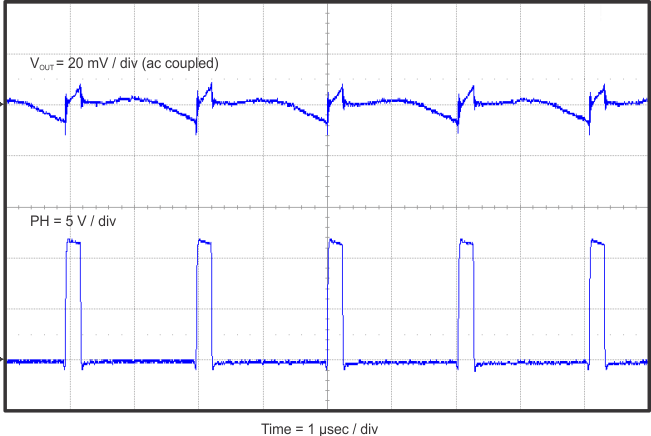
GUID-0A9A9641-C029-4C4F-935D-1FA7A7C0AA43-low.gifFigure 2-8 TPS56921EVM-188 Output Ripple