SLVU895B March 2013 – January 2022 LMZ31704 , LMZ31707 , LMZ31710
8 PCB Layout
Figure 8-1 through Figure 8-6 show the PCB layouts of the EVM.
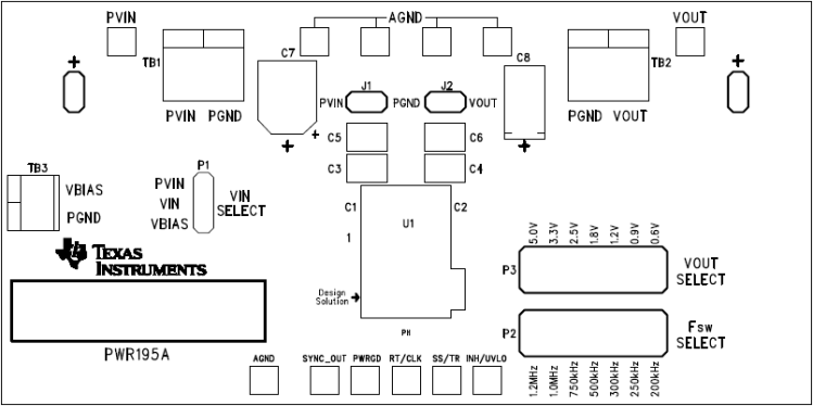 Figure 8-1 LMZ317xxEVM Topside Component Layout
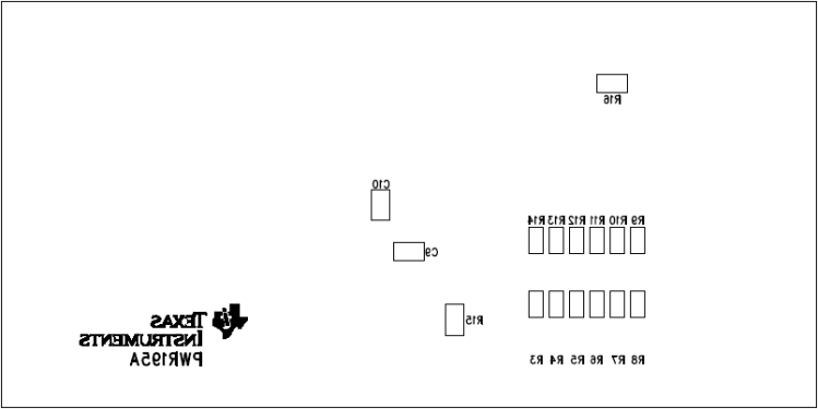 Figure 8-2 LMZ317xxEVM Bottom-Side Component Layout
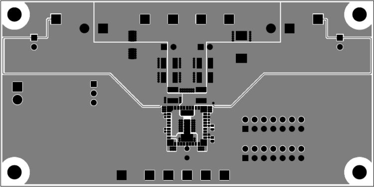 Figure 8-3 LMZ317xxEVM Layer 1 Copper
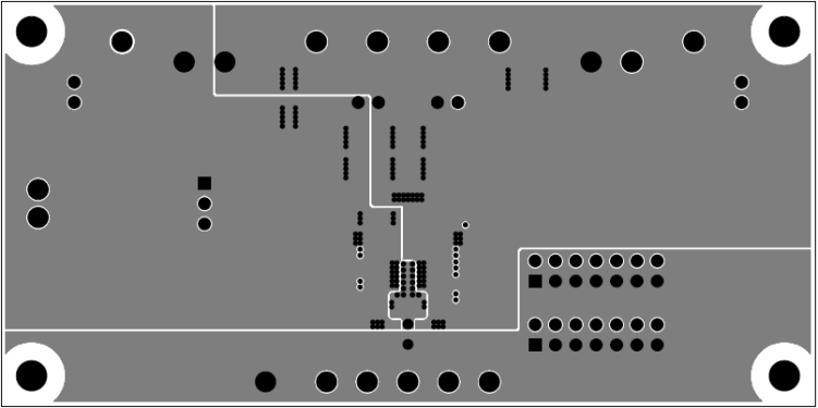 Figure 8-4 LMZ317xxEVM Layer 2 Copper
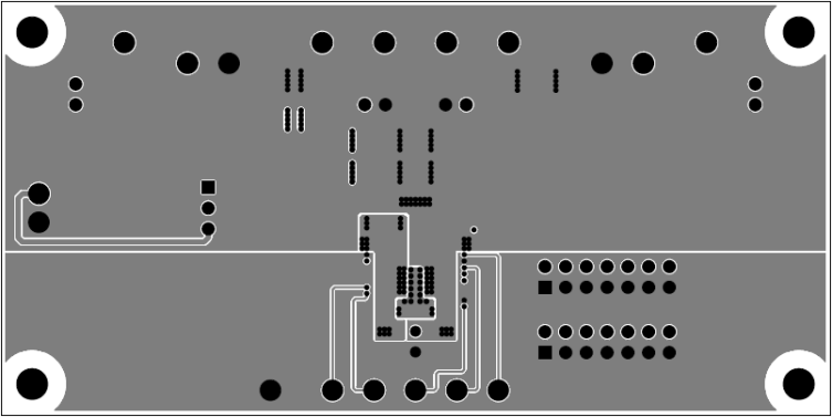 Figure 8-5 LMZ317xxEVM Layer 3 Copper
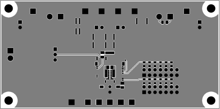 Figure 8-6 LMZ317xxEVM Layer 4 Copper