SLVU957A September 2019 – November 2021 BQ76922
- Trademarks
- 1Features
- 2BQ76922EVM Quick Start Guide
- 3Interface Adapter
- 4Battery Management Studio Software
- 5BQ76922EVM Circuit Module Use
- 6BQ76922EVM Circuit Module Physical Construction
- 7Related Documents from Texas Instruments
- 8Revision History
6.1 Board Layout
The BQ76922EVM circuit module is a 3.0-inch × 4.9-inch 4-layer circuit card assembly. It is designed for easy assembly with cell connections on the left edge to a terminal block. Pack terminals are on the top edge using a terminal block. Wide trace areas are used reducing voltage drops on the high current paths. Optional connections for hardware feature pins are on a separate terminal block on the top edge of the board. An on-board interface adapter with USB connector is located in the right lower corner. Configuration headers are toward the right side of the board. Pushbutton switches for wake up and reset of the BQ76922 are located near the bottom edge of the board. The EVM layout and construction allows easy understanding of the connections and access to the test points for evaluation, but the connector area and programming features result in a large board.
The board layout includes spark gaps with the reference designator prefix E. These spark gaps are fabricated with the board and no component is installed.
See additional information in the configuration and operation sections of this document. Figure 6-1 to Figure 6-8 show the board layout.
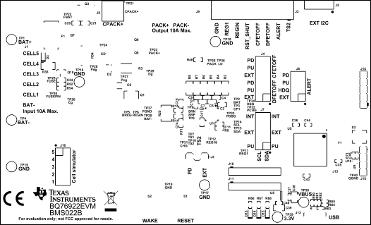 Figure 6-1 Top Silk
Screen
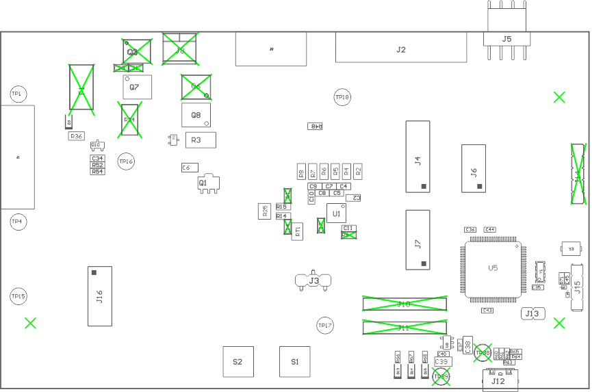 Figure 6-2 Top
Assembly
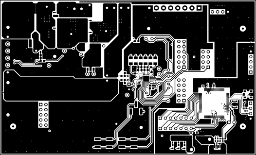 Figure 6-3 Top
Layer
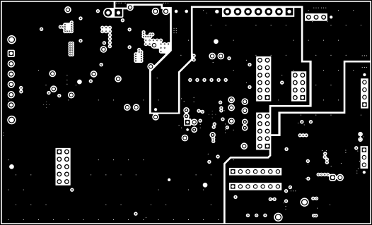 Figure 6-4 Layer
2
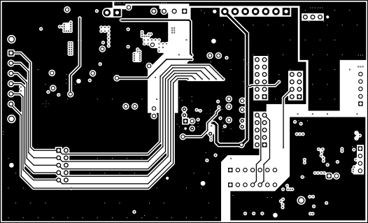 Figure 6-5 Layer
3
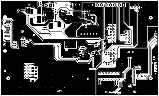 Figure 6-6 Bottom
Layer
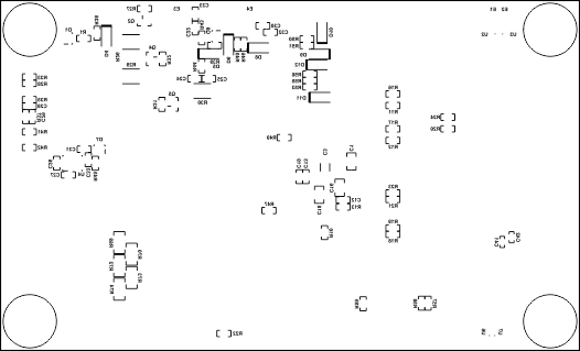 Figure 6-7 Bottom
Silk Screen
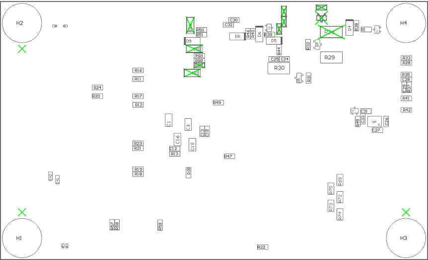 Figure 6-8 Bottom
Assembly