SLVUA03A December 2013 – May 2021 TPS65261-1
3 Bench Test Setup Conditions
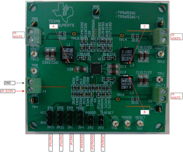
 Figure 3-1 Headers Description and Jumper Placement
Test points:
A: LX of VOUT1
B: LX of VOUT2
C: LX of VOUT3
VOUT1, VOUT2, VOUT3, VIN, PGOOD, RESET, V7V
Table 3-1 Input/Output Connection
| Number | Function | Description |
|---|---|---|
| J1 | BUCK1 connector | Output of BUCK1 |
| J2 | BUCK2 connector | Output of BUCK2 |
| J3 | BUCK3 connector | Output of BUCK3 |
| J4 | VIN connector | Apply power supply to this connector. |