SLVUBU5A May 2020 – December 2020 LM7481-Q1
- Trademarks
- 1Introduction
-
2Description
- 2.1 Input Power and Load (J1/J3 and J2/J4):
- 2.2 Enable Control (J5):
- 2.3 Over Voltage Protection (J6):
- 2.4 Input Voltage Monitor (J10 and VIN_MON):
- 2.5 Two Back-Back Connected MOSFETs (Q1/Q3 and Q2/Q4):
- 2.6 Output Slew Rate Control (R2 and C4):
- 2.7 Output Schottky Diode (D2) and LED Indication:
- 2.8 TVS Selection for 12-V Battery Protection:
- 2.9 TVS Selection for 24-V Battery Protection:
- 2.10 RC Input Snubber Option (R7 and C15):
- 2.11 Optional LC Filter at the Output (L2 and C11):
- 2.12 Test Points:
- 3Schematic
- 4Test Equipment Requirements
- 5Test Setup and Results
- 6EVM Board Layout and Bill of Materials
- 7Revision History
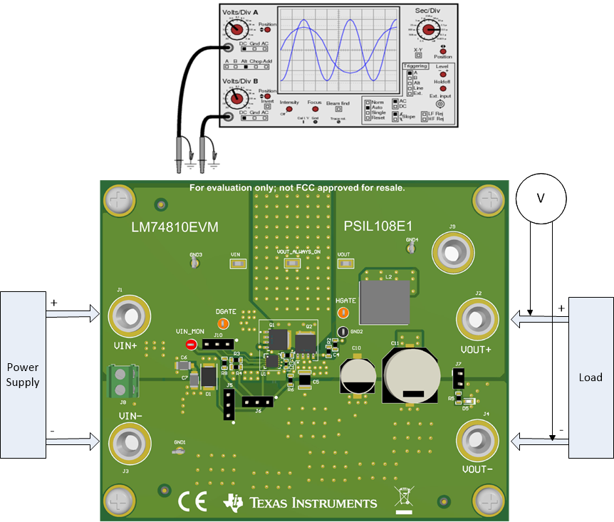
5 Test Setup and Results
This sections describes the test procedure for LM74810QDRRRQ1 device.
Default jumper setting for LM74810EVM board is shown in Table 5-1.
Table 5-1 Default Jumper Setting for
LM74810EVM
| J5 | J6 | J7 | J10 |
|---|---|---|---|
| 1-2 or connect 2 to external enable control | 2-3, OVP to Input | 1-2, Output LED Indication | 2-3, Input Voltage Sense |
 Figure 5-1 LM74810EVM Test Setup