SLVUC46D March   2021  – November 2023


  1.   1
  2.   Abstract
  3.   Trademarks
  4. 1Introduction
    1. 1.1 Overview
      1. 1.1.1 Purpose and Scope
  5. 2Evaluation Hardware Overview
    1. 2.1 Connections Overview
    2. 2.2 Connection Details
      1. 2.2.1 Common Connectors and Headers Across all EVM Variants
      2. 2.2.2 MCU Reset and User Button
      3. 2.2.3 Communication Interfaces
      4. 2.2.4 Supply Input
      5. 2.2.5 Current Limit Header (RIPROPI)
      6. 2.2.6 Device Signal and Control Header
      7. 2.2.7 Device Signal Test Points
    3. 2.3 LED Indicators
    4. 2.4 Headers and Connectors (Hardware Device Variant)
    5. 2.5 Headers and Connectors (SPI variant)
  6. 3EVM GUI Control Application
    1. 3.1 MSP430 FET Drivers
    2. 3.2 Cloud-based GUI
    3. 3.3 Local Installation
  7. 4EVM GUI Operation
    1. 4.1 Hardware Setup
    2. 4.2 Launching the DRV824x_DRV814x-Q1EVM GUI Application
    3. 4.3 Using the DRV824x_DRV814x-Q1EVM GUI Application
      1. 4.3.1 Register Map Page (SPI Device Variant)
      2. 4.3.2 Driver Control Page (SPI Device Variant)
      3. 4.3.3 Driver Control Page (HW Device Variant)
      4. 4.3.4 Updating Firmware
  8. 5Revision History

Device Signal and Control Header

The J4 header Figure 2-6 is provided for users who wany to interface an external control design and is also a convenient means for probing all device control signals. When interfacing with an external control design, remove the associated 0-ohm resistors immediately adjacent to the silk screen label.

Note: PH/IN2 signal is not present on DRV814x-Q1EVM variants. Refer to the EVM schematic for more details.
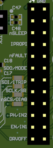
GUID-20230926-SS0I-FFHV-HLRJ-RQWFTHJZLWXZ-low.png Figure 2-6 DRV824x-Q1EVM Signal and Control Header