SLVUCC7A January   2022  – September 2022 TPS629211-Q1


  1.   Abstract
  2.   Trademarks
  3. 1Introduction
  4. 2Performance Specification
  5. 3EVM Configuration and Modification
    1. 3.1 Input and Output Capacitors
    2. 3.2 Configurable Enable Threshold Voltage
    3. 3.3 MODE/S-CONF Setting
    4. 3.4 Power Good
    5. 3.5 Power Good Pullup Voltage
    6. 3.6 Feedforward Capacitor Option
    7. 3.7 Output Voltage Setting
    8. 3.8 Loop Response Measurement
  6. 4EVM Test Setup
    1. 4.1 Input and Output Connectors
    2. 4.2 Jumper Configuration
      1. 4.2.1 JP1 Enable
      2. 4.2.2 JP2 MODE/S-CONF
      3. 4.2.3 JP3 Power Good
      4. 4.2.4 JP4 PG Pullup Voltage
  7. 5Test Results
  8. 6Board Layout
  9. 7Schematic and Bill of Materials
    1. 7.1 Schematic
    2. 7.2 Bill of Materials
  10. 8References
  11. 9Revision History

Board Layout

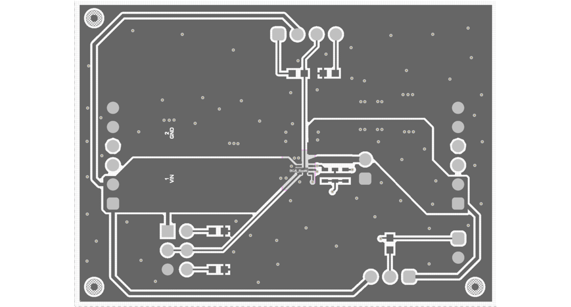
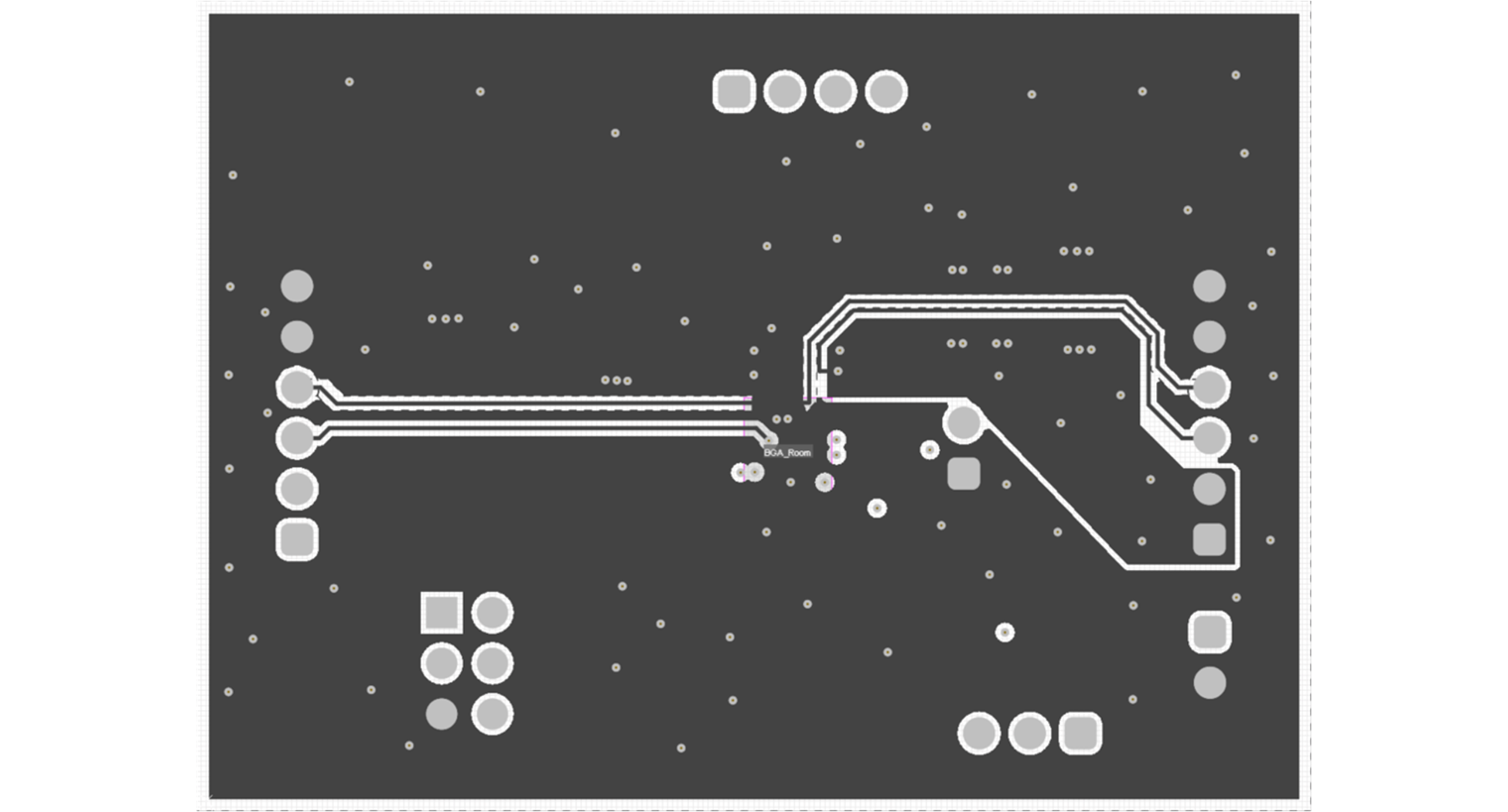
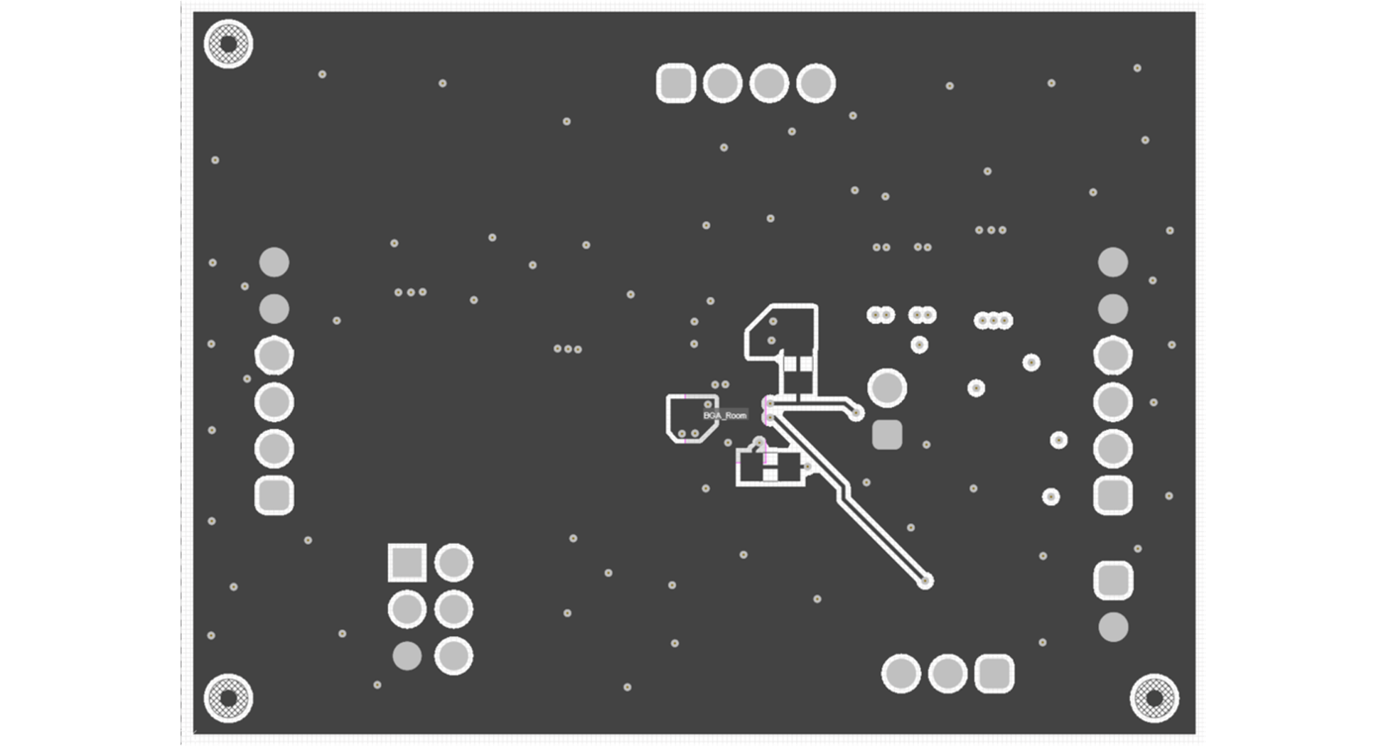
This section provides the EVM board layout and illustrations.
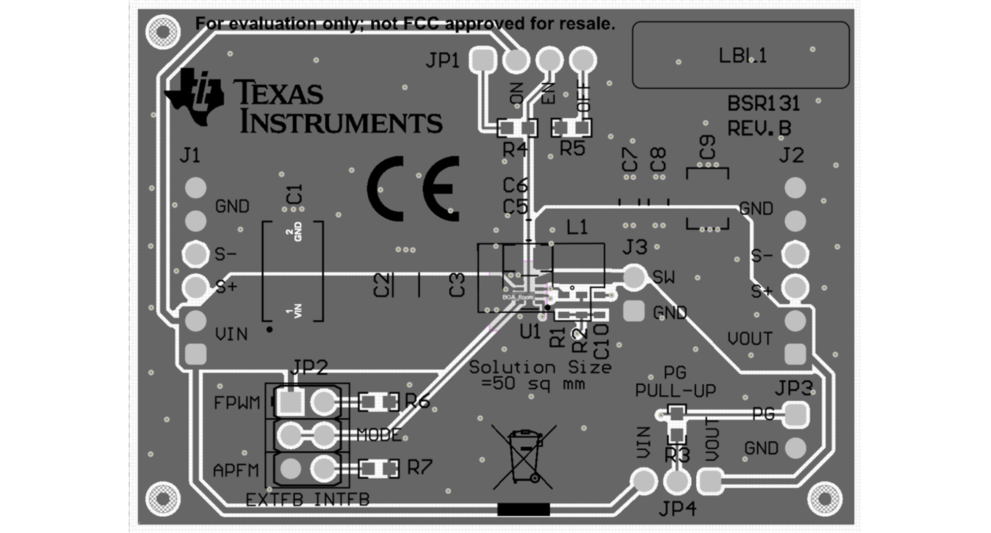
GUID-826C8815-4D37-451A-972E-A7B77153A2B9-low.pngFigure 6-1 Top Assembly
GUID-E9C571EB-4F71-4898-9C4B-84A2FC383573-low.pngFigure 6-2 Top Layer
GUID-8011C080-3B86-4A04-A222-E590C2C8AC4B-low.pngFigure 6-3 Internal Layer 1
GUID-03DEBD2D-351D-4094-A363-5E3977211D64-low.pngFigure 6-4 Internal Layer 2
GUID-85E39F90-ECE2-4BAF-B690-61DB33A81423-low.pngFigure 6-5 Bottom Layer