SLVUCE1A march 2023 – august 2023 TPS56837
3.1 Output Voltage Setpoint
To change the output voltage of the EVMs, change the value of resistor R6 (RFB_TOP) and resistor R7 (RFB_BOT). Changing the value of R6 and R7 can change the output voltage above 0.6 V. The value of R6 and R7 for a specific output voltage can be calculated using Equation 1.
Equation 1. 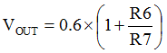
Table 3-1 lists the R6 and R7 values for some common output voltages.
Table 3-1 Recommended Component Values
Switching Frequency (kHz) | Output Voltage(1) (V) | R6(2) (kΩ) | R7 (kΩ) | L1 (µH) | COUT(3) (µF) | C10 (4)(pF) |
|---|---|---|---|---|---|---|
| TYP | ||||||
500 | 1.05 | 7.5 | 10 | 1 | 68 | |
| 1.8 | 20 | 10 | 1.5 | 68 | ||
| 3.3 | 45.3 | 10 | 2.2 | 62 | 150 | |
| 5 | 73.2 | 10 | 3.3 | 35 | 150 | |
9 | 140 | 10 | 4.7 | 22 | 100 | |
12 | 383 | 20 | 5.6 | 17 | 30 | |
800 | 1.05 | 7.5 | 10 | 0.68 | 68 | |
1.8 | 20 | 10 | 1 | 68 | ||
3.3 | 45.3 | 10 | 1.5 | 62 | 150 | |
5 | 73.2 | 10 | 2.2 | 35 | 150 | |
9 | 140 | 10 | 3.3 | 22 | 100 | |
12 | 383 | 20 | 3.3 | 17 | 30 | |
1200 | 1.05 | 7.5 | 10 | 0.47 | 68 | |
1.8 | 20 | 10 | 0.68 | 68 | ||
3.3 | 45.3 | 10 | 1 | 62 | 150 | |
5 | 73.2 | 10 | 1.5 | 35 | 150 | |
9 | 140 | 10 | 2.2 | 22 | 100 | |
12 | 383 | 20 | 2.2 | 17 | 30 |
(1) Please use the recommended L1 and COUT combination of the higher and closest output rail for unlisted output rails.
(2) R6 = 0 Ω for VOUT = 0.6 V.
(3) COUT is the sum of effective output capacitance. In this data sheet,
the effective capacitance is defined as the actual capacitance under DC bias
and temperature, not the rated or nameplate values. All high value ceramic
capacitors have a large voltage coefficient in addition to normal tolerances
and temperature effects. A careful study of bias and temperature variation
of any capacitor bank must be made to verify that the minimum value of
effective capacitance is provided. Refer to the information of DC bias and
temperature characteristics from manufacturers of ceramic capacitors.
(4) R8 and C10 can be used to improve the load transient response or improve the loop-phase margin. The Optimizing Transient Response of Internally Compensated DCDC Converters with Feed-forward Capacitor application report is helpful when experimenting with a feed-forward capacitor.