SLVUCF2 March   2022 TPS55289


  1.   Trademarks
  2. 1Introduction
    1. 1.1 Performance Specification
    2. 1.2 Modification
      1. 1.2.1 Modification
  3. 2Connector, Test Point, and Jumper Descriptions
    1. 2.1 Connector and Test Point Descriptions
    2. 2.2 Jumper Configuration
      1. 2.2.1 JP1 (ENABLE)
      2. 2.2.2 JP6 (SYNC)
      3. 2.2.3 JP7 (I2C Target Address Selection)
      4. 2.2.4 JP8 (Internal or External VCC Selection)
      5. 2.2.5 JP9 and JP10 (External Feedback and Internal Feedback Selection)
  4. 3Test Procedure
  5. 4Software User Interface
    1. 4.1 Install USB2ANY Explorer
    2. 4.2 GUI Installation
    3. 4.3 Interface Hardware Setup
    4. 4.4 User Interface Operation
    5. 4.5 Register Map Screen
  6. 5Schematic, Bill of Materials, and Board Layout
    1. 5.1 Schematic
    2. 5.2 List of Materials
    3. 5.3 Board Layout

JP9 and JP10 (External Feedback and Internal Feedback Selection)

The JP9 jumper is for the external feedback or the internal feedback selection. By default, this jumper is set to the FB_INT position. Place this jumper in the FB_EXT position for the external output voltage feedback.

The JP10 jumper is for the external feedback connection. Place a jumper across JP10 when using external feedback. Leave JP10 open when uses internal feedback.

When using external output voltage feedback, the output voltage is determined by Equation 1:

Equation 1. GUID-2E067DF5-4ED5-479B-BFE9-4683EFC3FEA0-low.gif

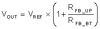
It is recommended to use 100 kΩ for the up resistor, RFB_UP. The reference voltage, VREF, at the FB/INT pin is programmable from 45 mV to 1.2 V by writing a 11-bit data into registers 00H and 01H.