SLVUCK9A august   2023  – august 2023


  1.   1
  2.   Description
  3.   Trademarks
  4. 1 Features
  5. 2 Applications
  6. 3 Hardware Image
  7. 4 Evaluation Module Overview
    1. 4.1 Introduction
    2. 4.2 Kit Contents
    3. 4.3 Reference
    4. 4.4 Device Information
  8. 5 Performance Specification Summary
  9. 6 Output Voltage Setpoint
  10. 7 Test Setup and Results
    1. 7.1 Input, Output Connections
    2. 7.2 Start-Up Procedure
    3. 7.3 Efficiency
    4. 7.4 Load Regulation
    5. 7.5 Line Regulation
    6. 7.6 Load Transient Response
    7. 7.7 Start-Up
    8. 7.8 Shutdown
    9. 7.9 Output Voltage Ripple
  11. 8 Hardware Design Files
    1. 8.1 Schematic
    2. 8.2 Layout
    3. 8.3 Bill of Materials
  12. 9 Reference
  13. 10Revision History

Start-Up

Figure 7-12 shows the TPS562203EVM start-up waveform relative to VIN. The load is 2 A.
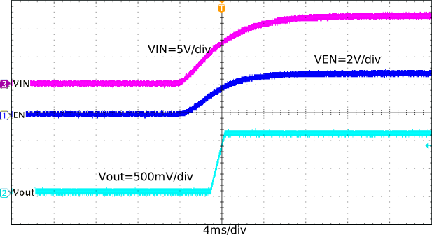
GUID-20230209-SS0I-MTML-FCNW-KFFXT7G5VQSP-low.svg Figure 7-10 TPS562203EVM Start-Up Relative to VIN

Figure 7-13 shows the TPS562203EVM start-up waveform relative to enable (EN). The load is 2 A.
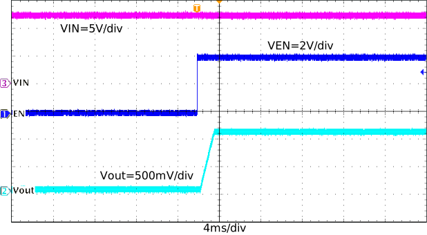
GUID-20230209-SS0I-ZZ1Z-LMB9-NTFW9ZNKRXQG-low.svg Figure 7-11 TPS562203EVM Start-Up Relative to EN