SLVUDL8 February 2026
2.2.1 EVM Setup
This section describes the typical setup and operation of the EVM for device evaluation. Typical EVM Test Setup shows a typical test configuration for operating the ISOW3080DWEEVM using two power supplies.
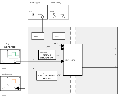 Figure 2-2 Typical EVM Test Setup
ISOW3080DWEEVM has many DNP resistors which can be populated or unpopulated along with 3-pin jumper options to setup the EVM to desired operating test conditions. Component Configurations lists and describes all the possible test configurations that can be achieved by populating various resistors and jumper options.
Table 2-1 Component
Configurations
| Component | Description |
|---|---|
| R1 | The resistor connects LDOs U1, U2 inputs together allowing only one power supply to be used instead of two power supplies. |
| R2, R15, R18 | Populating R15 bypasses LDO U1 allowing VDD to be powered directly from external power supply. When R15 is populated, R2 and R18 needs to be unpopulated to disconnect the LDO. When LDO is not bypassed, the recommended input voltage to LDO is between 9V and 12V |
| R5, R7, R9, R11, R13 | Sets LDO U1 output voltage to 5V or 3.3V for VDD1. Populate only R5 and R9 with 0Ω resistors to set LDO U1 output voltage to 5V. Populate only R7, R11 and R13 with 0Ω resistors to set LDO U1 output voltage to 3.3V(Default Configuration). |
| R3, R16, R19 | Populating R16 bypasses LDO U2 allowing VDDL to be powered directly from external power supply. When R16 is populated, R3 and R19 needs to be unpopulated to disconnect the LDO. When LDO is not bypassed, the recommended input voltage to LDO is between 9V and 12V. |
| R4, R6, R8, R10, R12, R14 | Sets LDO U2 output voltage to 5V or 3.3V or 2.5V for VDDL. Populate only R4 and R10 with 0Ω resistors to set LDO U2 output voltage to 5V. Populate only R6, R12 and R14 with 0Ω resistors to set LDO U2 output voltage to 3.3V(Default Configuration). Populate only R8, R12 and R14 with 0Ω resistors to set LDO U2 output voltage to 2.5V. |
| R17 | The resistor connects oscillator U3 output signal to U4 input D of ISOW3080, allowing EVM to be tested using a test signal without needing any external test signal input. |
| R20, R21 | Populating R20 sets U3 output signal rate to 500Kbps(Default Configuration) and populating R21 sets the rate to 12Mbps. |
| R30, R31 | These resistors allow shorting Y/Z and A/B on EVM to enable half-duplex configuration out of the full-duplex capable device. |
| L10, L11 | Common-Mode Choke(CMC) on RS485 bus. If populating L10 then remove R26 and R27. If populating L11 then remove R28 and R29. |
| R26, R27, R28, R29 | Populating R26 and R27 bypasses the CMC L10 on A/B Populating R28 and R29 bypasses the CMC L11 on Y/Z |
| R32, R34, R35, R37 | Optional footprints for external fail safe biasing. ISOW3080 has internal failsafe biasing enabled, hence DNP. |
| R38, R39, R40, R41 | Populate these for split termination configuration on A/B and Y/Z. |
| C32, C33 | Populate these for split termination configuration on A/B and Y/Z. |
| D1, D2 | Optional SOT-23 footprints for TVS Diode installation. |
| R42, R43 | Optional resistors which can be populated to extract ILOAD from VISOOUT when RS485 is not in use. Do not populate when using RS485 functionality. |
| C18. C19, C20, C21 | Optional capacitors for noise filtering on digital signal lines on Side1. |
| J3 | Don't use jumper to connect any pins. This just acts as an additional probe point for probing output R of ISOW3080 |
| J4 | Connect this jumper between the middle pin and GND1 to tie the input D pin low. Connect this jumper between the middle pin and VDDL to tie the input D pin high. |
| J5 | Connect this jumper between the middle pin and GND1 to tie the DE pin low. The driver input is disabled when the DE pin is low. Connect this jumper between the middle pin and VDDL to tie the DE pin high. The driver input is enabled when the DE pin is high. |
| J6 | Connect this jumper between the middle pin and GND1 to tie the RE pin low. The receiver is enabled when the RE pin is low.. Connect this jumper between the middle pin and VDDL to tie the RE pin high. The receiver is disabled when the RE pin is high |
| J7 | Jumper option to power ON or OFF the U3 oscillator. |