SLVUDN6 December   2025


  1.   1
  2.   Description
  3.   Features
  4.   Applications
  5.   5
  6. 1Evaluation Module Overview
    1. 1.1 Introduction
    2. 1.2 Kit Contents
    3. 1.3 Specification
    4. 1.4 Device Information
  7. 2Hardware
    1. 2.1 Additional Images
      1. 2.1.1 Pin Configuration
    2. 2.2 Power Requirements
    3. 2.3 Input and Output SMA connectors
    4. 2.4 Jumper Information
    5. 2.5 Test Point connector
  8. 3Hardware Design Files
    1. 3.1 Schematics
    2. 3.2 PCB Layouts
    3. 3.3 Bill of Materials (BOM)
  9. 4Additional Information
    1. 4.1 Trademarks

PCB Layouts

The following figures show the PCB layout for the VCA710RGREVM.

VCA710RGR VCA710RGREVM Top
                                                  Layer Figure 3-2 VCA710RGREVM Top Layer
VCA710RGR VCA710RGREVM Second
                                                  Layer (Ground Plane) Figure 3-3 VCA710RGREVM Second Layer (Ground Plane)
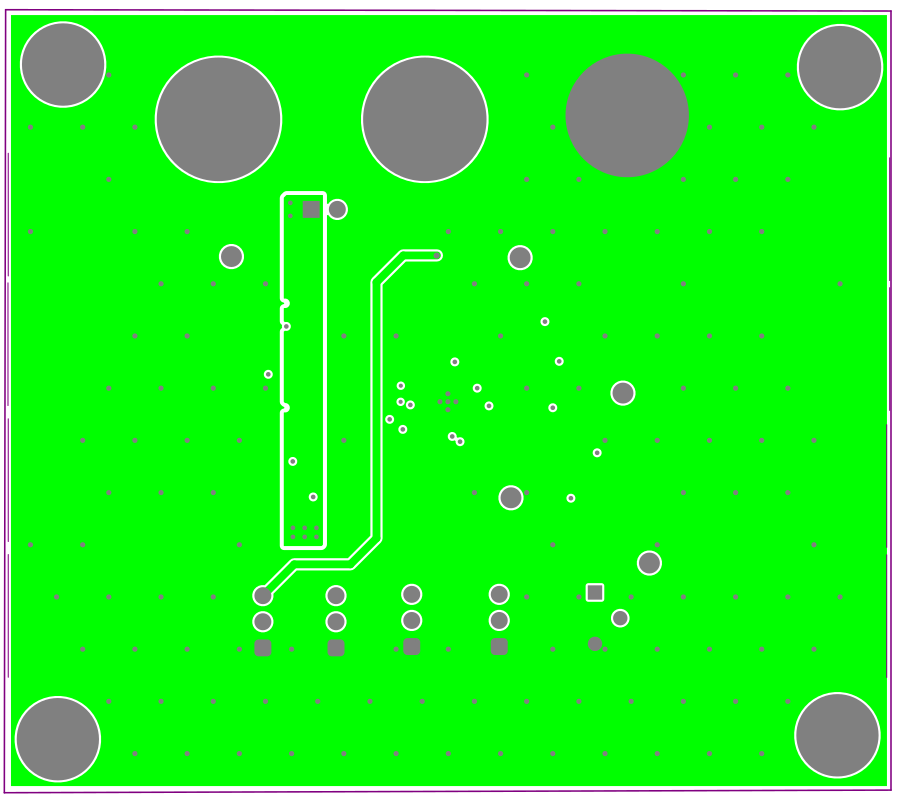
VCA710RGR VCA710RGREVM Third
                                                  Layer (Power Plane) Figure 3-4 VCA710RGREVM Third Layer (Power Plane)
VCA710RGR VCA710RGREVM Bottom
                                                  Layer Figure 3-5 VCA710RGREVM Bottom Layer