SLYT837 January 2023 TPS543B22 , TPS548A28 , TPS56121
3 Designing the second-stage filter
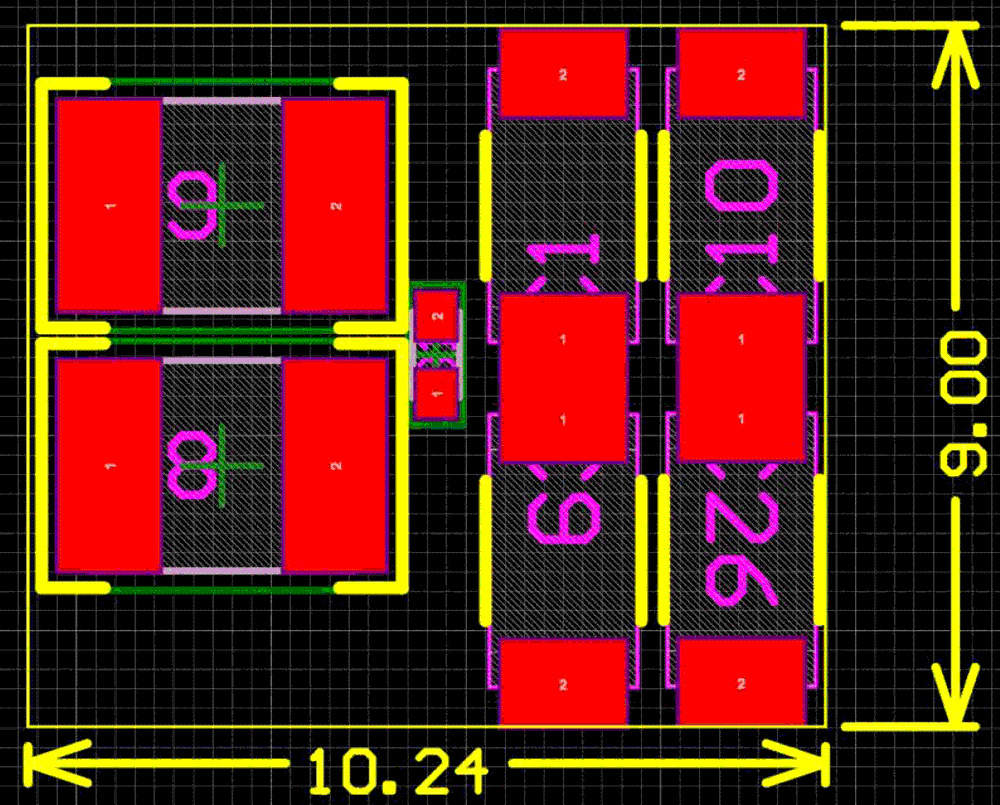
Even with low equivalent series resistance (ESR) ceramic output capacitors, it is not practical to use a buck converter’s inductor and capacitor (LC) output filter to achieve low output voltage ripple. Designers will likely need to use a second-stage LC filter in order to achieve output ripple below 5-mV. For more information about the design of a second-stage filter or the ripple measuring techniques, please see resources section. The value of the inductor of the second-stage filter can be calculated using Equation 1 and solving for L2. The inductor L2 is the second-stage inductor, C1 is the primary-stage output capacitor of the buck converter, and C2 is the second-stage capacitor network. For all three designs, the same second-stage filter was used (as shown in Table 3-1), occupying a circuit board area of 92mm2 (as shown in Figure 3-1).
| Part Number | Control Architecture | Switching Frequency | Second-Stage Inductance | Second-Stage Capacitance |
|---|---|---|---|---|
| TPS548A28 | D-CAP3 | 800 kHz | 2 x 0.68 µH | 4x 100 µF + 0.1 µF |
| TPS543B22 | ACM | 1000 kHz | 2 x 0.68 µH | 4x 100 µF + 0.1 µF |
| TPS56121 | Voltage-Mode | 500 kHz | 2 x 0.68 µH | 4 x 100 µF + 0.1 µF |
 Figure 3-1 Circuit board area of
second-stage filter at 92mm2.
Figure 3-1 Circuit board area of
second-stage filter at 92mm2.Once the second-stage inductor value (L2) is chosen and the components are assembled, the next step is to re-compensate the DC/DC converter’s control loop with the addition of the second-stage inductance and capacitance to ensure stability. It is important to mention that each control architecture has its own unique technique to re-compensate the control loop after adding the second stage filter, if needed. The output voltage ripple, efficiency penalty and stability of each control architecture were evaluated and then summarized the results.