SLYT837 January 2023 TPS543B22 , TPS548A28 , TPS56121
5 D-CAP3 control architecture
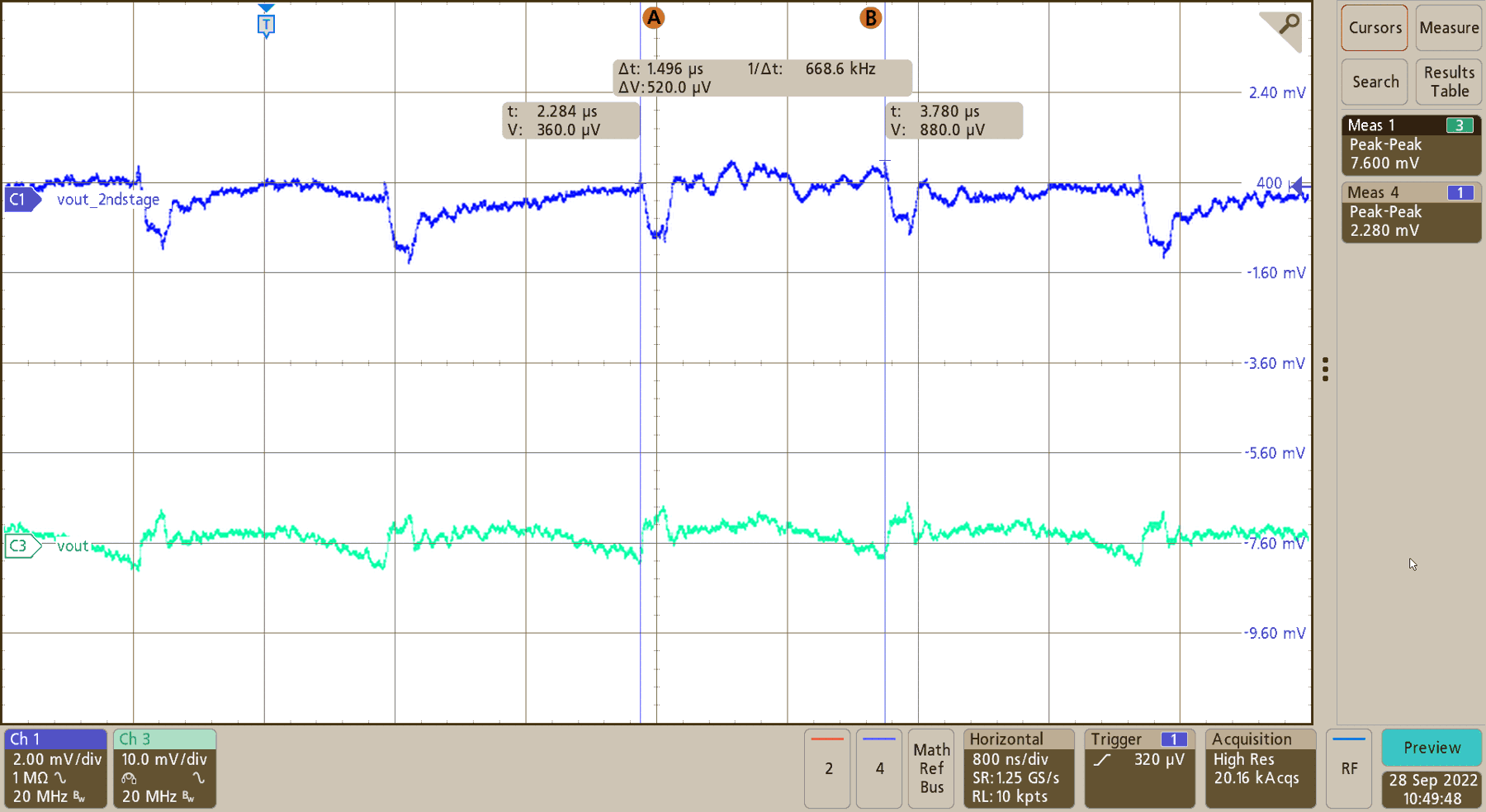
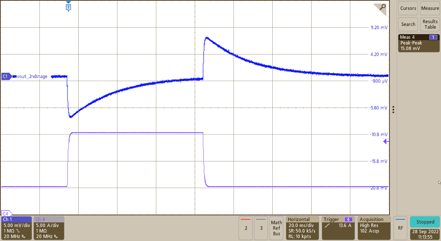
D-CAP3 uses a one-shot timer to generate an on-time pulse that is proportional to the input voltage and the output voltage. When the falling feedback voltage equals the reference voltage, a new PWM on-pulse is generated. The ramp is emulated by the output inductor. A signal from an internal ripple-injection circuit is fed directly into the comparator with its offset voltage eliminated, reducing the need for output voltage ripple from the capacitor’s ESR. One advantage of D-CAP3 and other constant on-time converters is additional loop compensation circuitry is not required. But, the control loop may have the ability adjusted by an adjustable ramp, if the device supports this feature, and the addition of feed forward capacitance at the output voltage feedback resistor divider network. The TPS548A28 output voltage peak-to-peak ripple without an additional filter is 7.6-mV. With the additional filter applied, the output voltage ripple is 2.3-mV (as shown in Figure 5-1). In this case, the TPS548A28 design required no adjustments to ensure stability. Figure 5-2 shows a load transient waveform with the same 10-A load-step as the previous converter, and the output voltage waveform after the implementation of the second-stage filter shows no sign of instability.
 Figure 5-1 TPS548A28 output voltage
ripple with and without additional second-stage filter.
 Figure 5-2 Transient response of
TPS548A28 using D-CAP3 control.