SNAA291A May 2016 – April 2021 ADC32RF45 , LMX2582 , LMX2592
3 Designing for Lowest Jitter
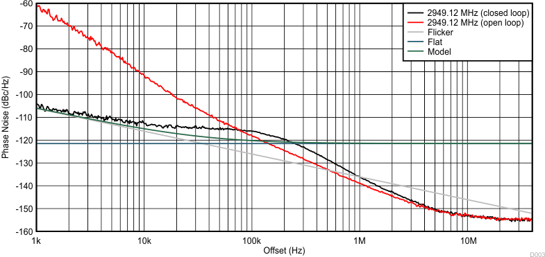
Now we focus on how to get the lowest possible jitter on the ADC clock source. Figure 3-1 shows a phase noise plot with output frequency at 2949.12 MHz. The black line is the closed loop (locked) phase noise and the red is the open loop (free running VCO) phase noise. Also, the PLL noise is modeled by a flicker noise component (gray line) and a flat PLL noise floor component (blue line). The sum of the two lines is the PLL noise. The loop bandwidth (where the phase noise starts to roll off) is around 100-kHz offset. If this loop bandwidth is low, the VCO noise pushes into the lower offset phase noise, and if the loop bandwidth is high, it can push the PLL phase noise into the VCO region. Generally, to design a loop filter for the lowest jitter, the point where the PLL noise model intersects the VCO is the optimal point (around 120 kHz in this example). This loop bandwidth is determined by the loop filter components of a clocking source, or in this case, an RF synthesizer (integrated PLL + VCO).
 Figure 3-1 Sampling Clock of 2949.12 MHz With 58 fs Jitter