SNAA361A april 2022 – may 2023 LMX2820
3 Standard LMX2820 Phase Noise Performance
To understand the performance improvement with alternative topologies, first characterize the inherent LMX2820 performance using the internal VCO. The TIDA-010230 reference design incorporates two LMX2820 synthesizers and includes options for operating in standard or alternative topologies. It is an ideal platform for comparing relative phase noise performance across different settings. Using the TIDA-010230 reference design, the LMX2820 is characterized with different PFD frequencies. Note, the LMX2820 PFD frequency is limited to 400 MHz maximum. It is expected that higher PFD frequencies that translate to lower N-divider values will provide better results.
The phase noise response and integrated jitter is dependent on the reference source. The reference source for the phase noise measurements is the SMA100B which is extremely good; however, it is conceivable that an even better reference source provides slightly improved results. The RMS jitter calculations start at 10 kHz to decouple a bit from the very low frequency offsets that are dominated by the reference performance.
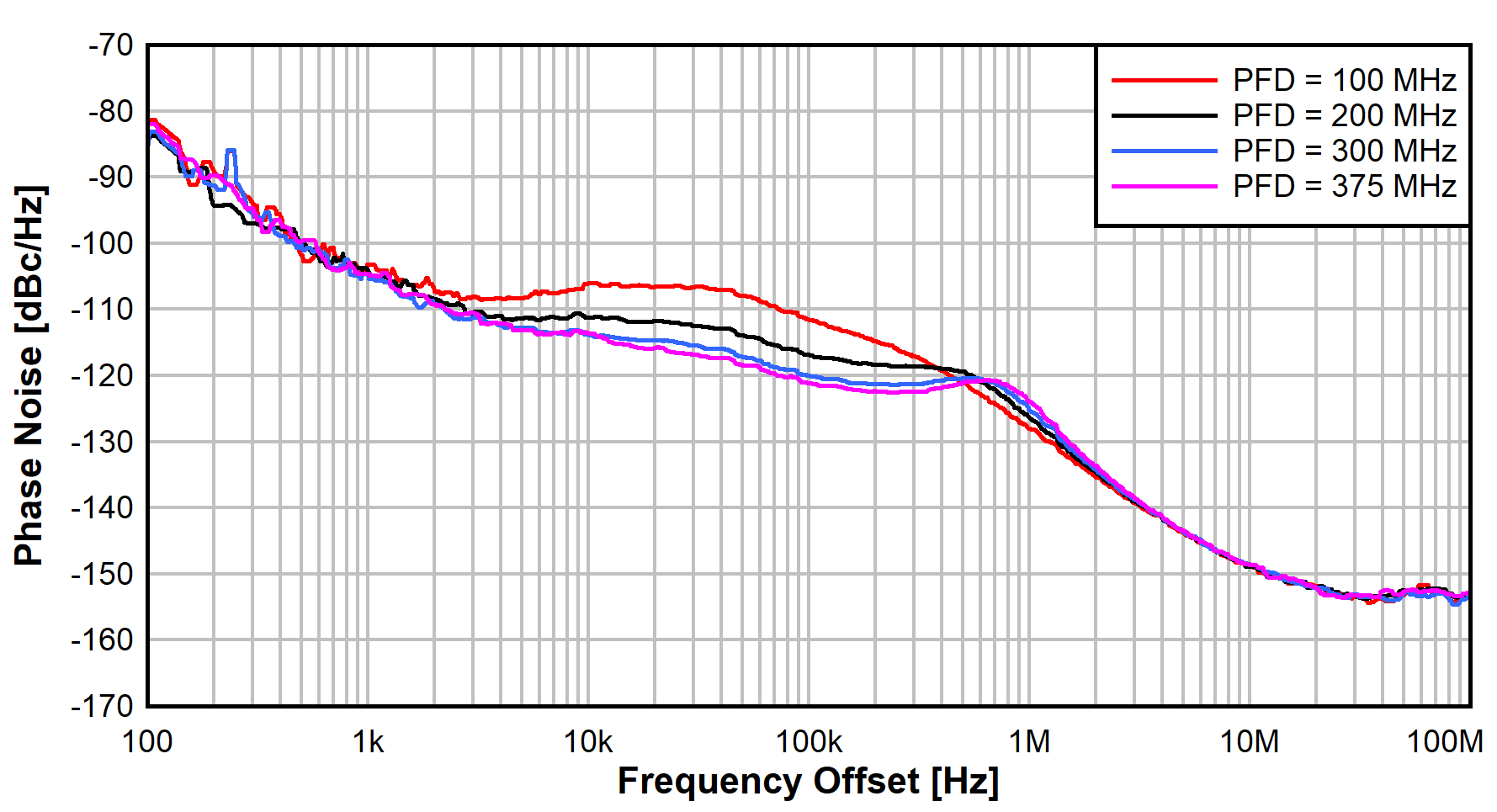
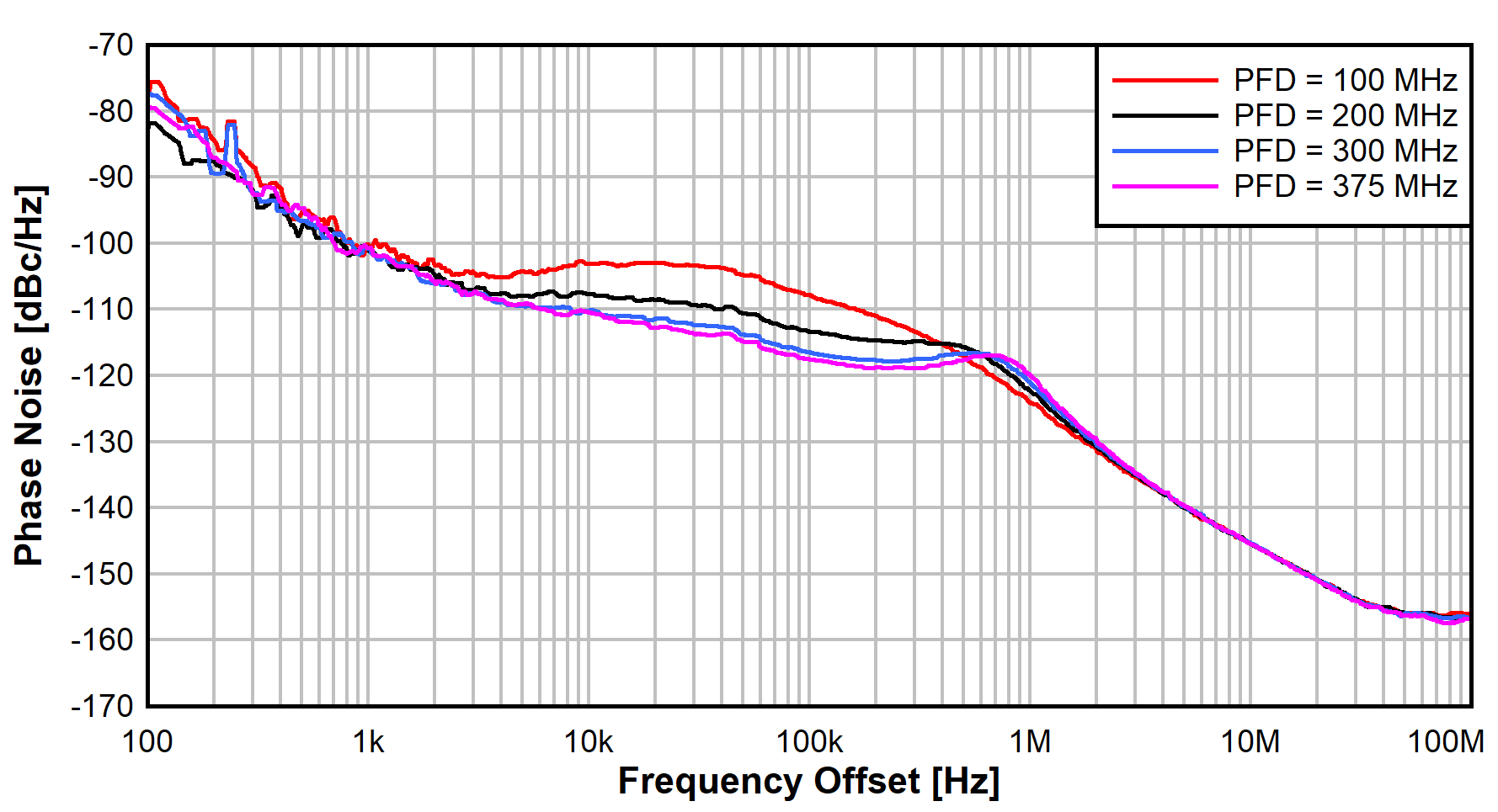
Figure 3-1 shows the phase noise performance of the LMX2820 with various PFD frequencies at 6-GHz output. RMS jitter is integrated from 10 kHz to 40 MHz. Similarly, Figure 3-2 shows the phase noise performance at 9 GHz measured after an RF amplifier to amplify the signal to around 10 dBm. The Agilent E5052 measured performance at frequencies below 7 GHz; the Rohde and Schwarz FSWP measured performance at the higher frequencies.
 Figure 3-1 LMX2820 Phase Noise Performance Over PFD Frequency at 6-GHz Output
 Figure 3-2 LMX2820 Phase Noise Performance Over PFD Frequency at 9-GHz Output
Table 3-1 shows the integrated RMS jitter for 6-GHz output and 9-GHz output. In all cases, the loop filter remains constant; there is some improvement possible with a lower PFD frequency if the loop filter is optimized for the required N-divider setting.
| 6 GHz | 9 GHz | |||
|---|---|---|---|---|
| PFD | N-Divider | Integrated Phase Noise | N-Divider | Integrated Phase Noise |
100 MHz | 60 | 62.4 fs | 90 | 61.5 fs |
200 MHz | 30 | 43.9 fs | 36 | 46.0 fs |
300 MHz | 20 | 38.1 fs | 30 | 40.5 fs |
375 MHz | 16 | 36.4 fs | 24 | 37.9 fs |
As expected, a higher PFD frequency corresponding to a lower N-divider value yields the best results. The optimum value is at 375 MHz which is convenient for locking to a 6-GHz or a 9-GHz VCO.
The area of the curve that shows the difference is the middle section from around 1k-Hz offset to 1-MHz offset. This area is heavily influenced by the PLL performance and correspondingly the N-divider setting. The reference source dominates the performance at very low-frequency offsets. The VCO performance dominates at high-frequency offsets. These areas do not change significantly with PFD changes.
For the subsequent measurements, the reference will be set at 375 MHz and the synthesizer set to 9-GHz output. A 9-GHz clock is convenient for clocking RF sampling data converters like the AFE7950 operating in S-band or X-band.