SNAS692A January 2017 – May 2017 LMK61E0M
PRODUCTION DATA.
- 1 Features
- 2 Applications
- 3 Description
- 4 Revision History
- 5 Pin Configuration and Functions
-
6 Specifications
- 6.1 Absolute Maximum Ratings
- 6.2 ESD Ratings
- 6.3 Recommended Operating Conditions
- 6.4 Thermal Information
- 6.5 Electrical Characteristics - Power Supply
- 6.6 3.3-V LVCMOS Output Characteristics
- 6.7 OE Input Characteristics
- 6.8 ADD Input Characteristics
- 6.9 Frequency Tolerance Characteristics
- 6.10 Frequency Margining Characteristics
- 6.11 Power-On/Reset Characteristics (VDD)
- 6.12 I2C-Compatible Interface Characteristics (SDA, SCL)
- 6.13 Other Characteristics
- 6.14 PLL Clock Output Jitter Characteristics
- 6.15 Additional Reliability and Qualification
- 6.16 Typical Characteristics
- 7 Parameter Measurement Information
-
8 Detailed Description
- 8.1 Overview
- 8.2 Functional Block Diagram
- 8.3
Feature Description
- 8.3.1 Device Block-Level Description
- 8.3.2 Device Configuration Control
- 8.3.3 Register File Reference Convention
- 8.3.4 Configuring the PLL
- 8.3.5 Integrated Oscillator
- 8.3.6 Reference Divider and Doubler
- 8.3.7 Phase Frequency Detector
- 8.3.8 Feedback Divider (N)
- 8.3.9 Fractional Engine
- 8.3.10 Charge Pump
- 8.3.11 Loop Filter
- 8.3.12 VCO Calibration
- 8.3.13 High-Speed Output Divider
- 8.3.14 High-Speed Clock Output
- 8.3.15 Device Status
- 8.4 Device Functional Modes
- 8.5 Programming
- 8.6
Register Maps
- 8.6.1
Register Descriptions
- 8.6.1.1 VNDRID_BY1 Register; R0
- 8.6.1.2 VNDRID_BY0 Register; R1
- 8.6.1.3 PRODID Register; R2
- 8.6.1.4 REVID Register; R3
- 8.6.1.5 SLAVEADR Register; R8
- 8.6.1.6 EEREV Register; R9
- 8.6.1.7 DEV_CTL Register; R10
- 8.6.1.8 XO_CAPCTRL_BY1 Register; R16
- 8.6.1.9 XO_CAPCTRL_BY0 Register; R17
- 8.6.1.10 CMOSCTL Register; R20
- 8.6.1.11 DIFFCTL Register; R21
- 8.6.1.12 OUTDIV_BY1 Register; R22
- 8.6.1.13 OUTDIV_BY0 Register; R23
- 8.6.1.14 RDIVCMOSCTL Register; R24
- 8.6.1.15 PLL_NDIV_BY1 Register; R25
- 8.6.1.16 PLL_NDIV_BY0 Register; R26
- 8.6.1.17 PLL_FRACNUM_BY2 Register; R27
- 8.6.1.18 PLL_FRACNUM_BY1 Register; R28
- 8.6.1.19 PLL_FRACNUM_BY0 Register; R29
- 8.6.1.20 PLL_FRACDEN_BY2 Register; R30
- 8.6.1.21 PLL_FRACDEN_BY1 Register; R31
- 8.6.1.22 PLL_FRACDEN_BY0 Register; R32
- 8.6.1.23 PLL_MASHCTRL Register; R33
- 8.6.1.24 PLL_CTRL0 Register; R34
- 8.6.1.25 PLL_CTRL1 Register; R35
- 8.6.1.26 PLL_LF_R2 Register; R36
- 8.6.1.27 PLL_LF_C1 Register; R37
- 8.6.1.28 PLL_LF_R3 Register; R38
- 8.6.1.29 PLL_LF_C3 Register; R39
- 8.6.1.30 PLL_CALCTRL Register; R42
- 8.6.1.31 NVMSCRC Register; R47
- 8.6.1.32 NVMCNT Register; R48
- 8.6.1.33 NVMCTL Register; R49
- 8.6.1.34 MEMADR Register; R51
- 8.6.1.35 NVMDAT Register; R52
- 8.6.1.36 RAMDAT Register; R53
- 8.6.1.37 NVMUNLK Register; R56
- 8.6.1.38 INT_LIVE Register; R66
- 8.6.1.39 SWRST Register; R72
- 8.6.1
Register Descriptions
- 9 Application and Implementation
- 10Power Supply Recommendations
- 11Layout
- 12Device and Documentation Support
- 13Mechanical, Packaging, and Orderable Information
9 Application and Implementation
NOTE
Information in the following applications sections is not part of the TI component specification, and TI does not warrant its accuracy or completeness. TI’s customers are responsible for determining suitability of components for their purposes. Customers should validate and test their design implementation to confirm system functionality.
9.1 Application Information
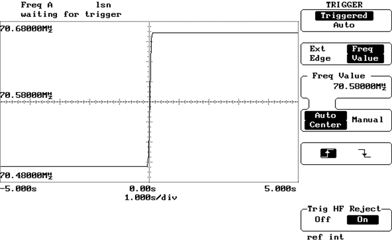
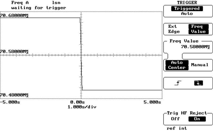
The LMK61E0 features fine and coarse frequency margining capabilities which allow it to be used in applications requiring the output frequency to be adjusted on the fly. In fractional PLL mode, the numerator of the PLL fractional feedback divider can be updated over I2C to update the output frequency without glitches or spikes, allowing the device to be used as a DCXO. The output frequency step size for every bit change in the numerator of the PLL fractional feedback divider is given in Configuring the PLL. The Application Curves section below illustrates the glitch-less switch in output frequency when the numerator is updated. The frequency margining features can also aid the hardware designer during the system debug and validation phase.
9.2 Typical Application
9.2.1 Design Requirements
Consider a typical digital subscriber line (DSL) application, in which a local modem must track the clock signal of a network modem to ensure accurate and efficient data transfer. In such systems, a DCXO is implemented to allow a local processor to digitally control the oscillator frequency to maintain synchronization. An example of such a clock frequency would be 70.656 MHz.
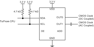
The typical schematic above shows the I2C connection to the processor and output configurations for AC or DC coupling. OE and ADD can be left floating. The internal pullup resistor on OE enables OUT0. Leaving ADD floating sets the LSB of the I2C slave address to 01.
The Detailed Design Procedure below describes the procedure to generate and adjust the required output frequency for the above scenario using LMK61E0M.
9.2.2 Detailed Design Procedure
This design procedure will give a quick outline of the process of configuring the LMK61E0M in the above use case. Typically, the easiest approach to configuring the PLL is to start with the desired output frequency and work backwards.
- VCO Frequency Selection
- The first step is to calculate the possible VCO frequencies given the required output frequency of 70.656 MHz. The LMK61E0M output dividers consist of the VCO post divider that can be set to /4 or /5, and the output divider that can be set from /6 to /256. The VCO can output frequencies from 4.6 GHz to 5.6 GHz. Therefore, the output frequency multiplied by the total divide value must fall within this range.
- To determine the boundary of the total divide value, we can divide the VCO frequency limits by the output frequency, resulting in a range of 65.1 to 79.3. Any combination of dividers that result in a total divide value within this range will result in a valid VCO frequency. The possible divider combinations and the resulting VCO frequencies are listed in columns 1 and 2, respectively, of Table 4, below.
- Input Divider and Doubler/Phase Detector Frequency Configuration
- The next step is to set the reference divider and doubler in the reference frequency path to the PLL. The reference divider can be set to /1 or /4, and the doubler can be set to x1 or x2. The main trade-off is that a higher phase detector frequency will result in better output phase noise performance and a lower phase detector frequency will result in a finer output frequency step size when adjusting the feedback divider numerator in DCXO mode.
- In the DSL application, a finer step size is desired so the reference divider will be set to /4 and the doubler to x1 to minimize the phase detector frequency. The phase detector frequency can then be calculated by multiplying and dividing the reference frequency of 50 MHz by those values, resulting in 12.5 MHz.
- Note that in some applications, a trade-off in step size to obtain better phase noise performance is acceptable. In that case the design procedure can be continued, substituting the relevant reference divider and doubler configuration and phase detector frequency.
- Feedback Divider Selection
- The possible feedback divider values can then be calculated by dividing the VCO frequency by the phase detector frequency. The possible values are listed in column 3 of Table 4.
- Glitch-less frequency margining in DCXO mode is achieved by adjusting the numerator of the feedback divider without changing the integer value of the divider, which could cause a frequency glitch. Therefore, the output frequency tuning range is limited by which VCO frequency and feedback divider we select out of the valid combinations. To obtain as equal of a tuning range above and below the nominal output frequency as possible, a feedback divider value with fractional portion as close to 1/2 as possible should be chosen.
- The VCO frequency of 5369.856 MHz results in a feedback divider of 429.58848, which has a fractional portion closest to 1/2. The decimal converted to a fraction is 429+58848/100000. To minimize step size, the fraction can be converted to the maximum equivalent fraction of 2412768/4100000 as limited by the maximum denominator of 4194303.
- Frequency Margining
- With the device configured to output the nominal frequency of 70.656 MHz, the numerator can be adjusted over I2C to tune the output frequency.
- Using equation 3 in Configuring the PLL, the step size of this configuration can be calculated to be approximately 4x10⁻⁸ MHz or 0.58 ppb.
- The maximum and minimum tuning range limits can be determined by calculating the maximum shift in frequency from nominal without changing the integer portion of the feedback divider (including setting the numerator to zero or equal to the denominator). In this case, the limits are a maximum of +955 ppm and a minimum of –1365 ppm from nominal.
Table 4. PLL Configuration Options
| 1. POSSIBLE OUTPUT DIVIDER COMBINATIONS | 2. POSSIBLE VCO FREQUENCIES (MHz) | 3. FEEDBACK DIVIDER WITH PDF=12.5 MHz | 4. EQUIVALENT FRACTIONAL FEEDBACK DIVIDER VALUES |
|---|---|---|---|
| 68 (/4, /17) | 4804.608 | 384.36864 | 384+1511424/4100000 |
| 70 (/5, /14) | 4945.92 | 395.6736 | 395+2822384/4190000 |
| 72 (/4, /18) | 5087.232 | 406.97856 | 406+4012096/4100000 |
| 75 (/5, /15) | 5299.2 | 423.936 | 423+3925584/4194000 |
| 76 (/4, /19) | 5369.856 | 429.58848 | 429+2412768/4100000 |
9.2.2.1 PLL Loop Filter Design
The EVM software tool TICS Pro/Oscillator Programming Tool can be used to aid loop filter design. The Easy Configuration GUI is able to generate a suggested set of loop filter values given a desired output frequency. The tool recommends a PLL configuration that is designed to minimize jitter. As of the publication of this document, it is not yet able to optimize for desired tuning range in DCXO mode. When configuring the device for operation in DCXO mode, TI recommends using the software suggested loop filter settings as a starting point and then perform the procedure described in Detailed Design Procedure to optimize the PLL configuration to suit the application needs.
A general set of loop filter design guidelines are given below:
- There are many device configurations to achieve the desired output frequency from a device. However there are some optimizations and trade-offs to be considered.
- The guidelines below may be followed when configuring PLL related dividers or other related registers:
- For lowest possible in-band PLL flat noise, maximize phase detector frequency to minimize N divide value.
- For fractional divider values, keep the denominator at highest value possible to minimize spurs. It is also best to use a higher order modulator whenever possible for the same reason.
- As a rule of thumb, keep the phase detector frequency approximately between 10 × PLL loop bandwidth and 100 × PLL loop bandwidth. A phase detector frequency less than 5 × PLL bandwidth may be unstable.
- While designing the loop filter, adjusting the charge pump current or N value can help with loop filter component selection. Lower charge pump currents and larger N values result in smaller component values but may increase impacts of leakage and reduce PLL phase noise performance.
- A more detailed understanding of loop filter design can be found in Dean Banerjee's PLL Performance, Simulation, and Design.
9.2.2.2 Spur Mitigation Techniques
The LMK61E0M offers several programmable features for optimizing fractional spurs. To get the best out of these features, it makes sense to understand the different kinds of spurs as well as their behaviors, causes, and remedies. Although optimizing spurs may involve some trial and error, there are ways to make this process more systematic. TI offers the Clock Design Tool (SNAU082) for more information and estimation of fractional spurs.
9.2.2.2.1 Phase Detection Spur
The phase detector spur occurs at an offset from the carrier equal to the phase detector frequency, fPD. To minimize this spur, consider a lower phase detector frequency. In some cases where the loop bandwidth is very wide relative to the phase detector frequency, some benefit might be gained from using a narrower loop bandwidth or adding poles to the loop filter by using R3 and C3 if previously unused, but otherwise the loop filter has minimal impact. Bypassing at the supply pins and board layout can also have an impact on this spur, especially at higher phase detector frequencies.
9.2.2.2.2 Integer Boundary Fractional Spur
This spur occurs at an offset equal to the difference between the VCO frequency and the closest integer channel for the VCO. For instance, if the phase detector frequency is 100 MHz and the VCO frequency is 5003 MHz, then the integer boundary spur would be at 3-MHz offset. This spur can be either PLL or VCO dominated. If it is PLL dominated, decreasing the loop bandwidth and some of the programmable fractional words may impact this spur. If the spur is VCO dominated, then reducing the loop filter will not help, but rather reducing the phase detector and having good slew rate and signal integrity at the selected reference input will help.
9.2.2.2.3 Primary Fractional Spur
These spurs occur at multiples of fPD/DEN and are not the integer boundary spur. For instance, if the phase detector frequency is 100 MHz and the fraction is 3/100, the primary fractional spurs would be at 1 MHz, 2 MHz, 4 MHz, 5 MHz, 6 MHz, and so forth. These are impacted by the loop filter bandwidth and modulator order. If a small frequency error is acceptable, then a larger equivalent fraction may improve these spurs. This larger unequivalent fraction pushes the fractional spur energy to much lower frequencies that where they are not impactful to the system performance.
9.2.2.2.4 Sub-Fractional Spur
These spurs appear at a fraction of fPD/DEN and depend on modulator order. With the first order modulator, there are no sub-fractional spurs. The second order modulator can produce 1/2 sub-fractional spurs if the denominator is even. A third order modulator can produce sub-fractional spurs at 1/2, 1/3, or 1/6 of the offset, depending if it is divisible by 2 or 3. For instance, if the phase detector frequency is 100 MHz and the fraction is 3/100, no sub-fractional spurs for a first order modulator or sub-fractional spurs at multiples of 1.5 MHz for a second or third order modulator would be expected. Aside from strategically choosing the fractional denominator and using a lower order modulator, another tactic to eliminate these spurs is to use dithering and express the fraction in larger equivalent terms. Because dithering also adds phase noise, its level needs to be managed to achieve acceptable phase noise and spurious performance.
Table 5 summarizes spur and mitigation techniques.
Table 5. Spur and Mitigation Techniques
| SPUR TYPE | OFFSET | WAYS TO REDUCE | TRADE-OFFS |
|---|---|---|---|
| Phase Detector | fPD | Reduce Phase Detector Frequency. | Although reducing the phase detector frequency does improve this spur, it also degrades phase noise. |
| Integer Boundary | fVCO mod fPD | Methods for PLL Dominated Spurs | Reducing the loop bandwidth may degrade the total integrated noise if the bandwidth is too narrow. |
| - Avoid the worst case VCO frequencies if possible. | |||
| - Ensure good slew rate and signal integrity at reference input. | |||
| - Reduce loop bandwidth or add more filter poles to suppress out of band spurs. | |||
| Methods for VCO Dominated Spurs | Reducing the phase detector may degrade the phase noise. | ||
| - Avoid the worst case VCO frequencies if possible. | |||
| - Reduce Phase Detector Frequency. | |||
| - Ensure good slew rate and signal integrity at reference input. | |||
| Primary Fractional | fPD/DEN | - Decrease Loop Bandwidth. | Decreasing the loop bandwidth may degrade in-band phase noise. Also, larger unequivalent fractions don’t always reduce spurs. |
| - Change Modulator Order. | |||
| - Use Larger Unequivalent Fractions. | |||
| Sub-Fractional | fPD/DEN/k k=2,3, or 6 | - Use Dithering. | Dithering and larger fractions may increase phase noise. |
| - Use Larger Equivalent Fractions. | |||
| - Use Larger Unequivalent Fractions. | |||
| - Reduce Modulator Order. | |||
| - Eliminate factors of 2 or 3 in denominator. |
9.2.2.3 Device Programming
The EVM software tool TICS Pro/Oscillator Programming Tool can be used to program the device with the desired configuration. Simply select the Program EEPROM option and the software will automatically load the current configuration to EEPROM. The settings will then be available upon subsequent startup without the need to reload the registers over I2C.
9.2.3 Application Curves
 Figure 14. Increasing Output Frequency in DCXO Mode
 Figure 15. Decreasing Output Frequency in DCXO Mode
