SNAU263A February 2022 – July 2022
- Abstract
- Trademarks
- 1Introduction
- 2EVM Quick Start
- 3EVM Configuration
-
4EVM Schematics
- 4.1 Power Supply Schematic
- 4.2 Alternative Power Supply Schematic
- 4.3 Power Distribution Schematic
- 4.4 LMK5B33216 and Input Reference Inputs IN0 to IN1 Schematic
- 4.5 Clock Outputs OUT0 to OUT3 Schematic
- 4.6 Clock Outputs OUT4 to OUT9 Schematic
- 4.7 Clock Outputs OUT10 to OUT15 Schematic
- 4.8 XO Schematic
- 4.9 Logic I/O Interfaces Schematic
- 4.10 USB2ANY Schematic
- 5EVM Bill of Materials
- 6Appendix A - TICS Pro LMK5B33216 Software
- 7Revision History
6.4.1 APLL DCO
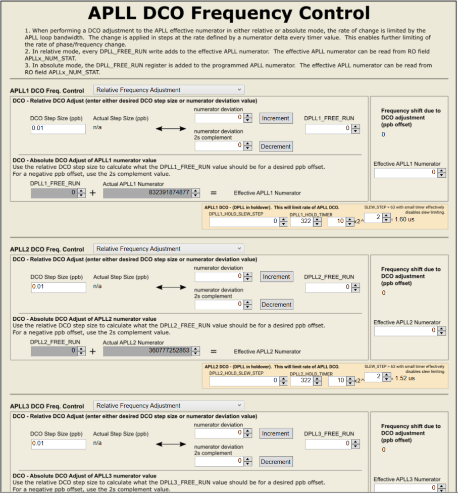
To use the DCO shift controls on a given APLL, enter the DCO ppb step value into the DCO Step Size (ppb) box shown below. The entered step size will be used to calculate a numerator deviation and a 2s complement numerator deviation. To perform the shift, the increment or decrement button must be pressed. An increment will write the numerator deviation to the DPLLx_FREE_RUN control which will result in a positive frequency shift in the amount specified by the DCO Step Size (ppb). An decrement will write the 2s complement numerator deviation to the DPLLx_FREE_RUN control which will result in a negative frequency shift in the amount specified by the DCO Step Size (ppb).
The slew rate at which the adjustment will occur is set on the DPLLx_HOLD_SLEW_STEP control. Ensure the DPLLx_HOLD_SLEW_STEP is NOT equal to 0, otherwise the adjustment will not occur. Recommended DPLLx_HOLD_SLEW_STEP value is 63 (maximum value). A value of 63 will result in the fastest adjustment.
 Figure 6-16 APLL DCO Controls.