SNAU298 October   2023


  1.   1
  2.   Description
  3.   Features
  4.   Applications
  5.   5
  6. 1Evaluation Module Overview
    1. 1.1 Introduction
    2. 1.2 Kit Contents
    3. 1.3 Specification
    4. 1.4 Device Information
  7. 2Hardware
    1. 2.1 EVM Quick Start
      1. 2.1.1 Hardware Setup
      2. 2.1.2 Measure
    2. 2.2 Device Operation Modes
    3. 2.3 EVM Configuration
      1. 2.3.1 Power Supply
      2. 2.3.2 Logic Input and Outputs
      3. 2.3.3 Clock Input
      4. 2.3.4 Clock Outputs
      5. 2.3.5 Status Outputs, LEDs, and Test Points
  8. 3Software
    1. 3.1 Software Installation
      1. 3.1.1 Software Setup
      2. 3.1.2 Program and Setup
    2. 3.2 TICS Pro LMKDB1120 Software
      1. 3.2.1 Input
        1. 3.2.1.1 Input Interface Type
        2. 3.2.1.2 Input Termination
        3. 3.2.1.3 Automatic Output Disable (AOD)
        4. 3.2.1.4 LOS Event
        5. 3.2.1.5 LOS Readback
      2. 3.2.2 Device Info
        1. 3.2.2.1 EVM Setup
        2. 3.2.2.2 SMBus
      3. 3.2.3 Output
        1. 3.2.3.1 SMBus
        2. 3.2.3.2 OE Pin Control
        3. 3.2.3.3 Side Band Interface (SBI)
  9. 4Implementation Results
    1. 4.1 Typical Phase Noise Characteristic
  10. 5Hardware Design Files
    1. 5.1 Schematics
    2. 5.2 PCB Layouts
    3. 5.3 Bill of Materials (BOM)
  11. 6Compliance Information
    1. 6.1 Compliance and Certifications
  12. 7References

Typical Phase Noise Characteristic

Figure 5-1 show the typical phase noise performance for 156.25 MHz reference clock input using a SMA100B.

LMKDB1120EVM was configured in cascaded mode to get these measurements:

  1. SMA100B → LMKDB1120EVM input. Then, LMKDB1120EVM to secondary LMKDB1120 EVM. This was done to get good slew rate at the input. Other methods like a clipping circuit can be used to get a desired slew rate and square wave form from the SMA100B.
  2. Outputs phase noise is measured through a Balun to convert the differential waveform from the LMKDB1120 into a single-ended waveform for a phase noise analyzer.

    As shown below in Figure 5-1, reference input jitter is 36.7 fs. As shown in Figure 5-2, measured jitter on the output of LMKDB1120 is 43.7 fs. Calculated typical additive jitter is about 24 fs for the LMKDB1120.
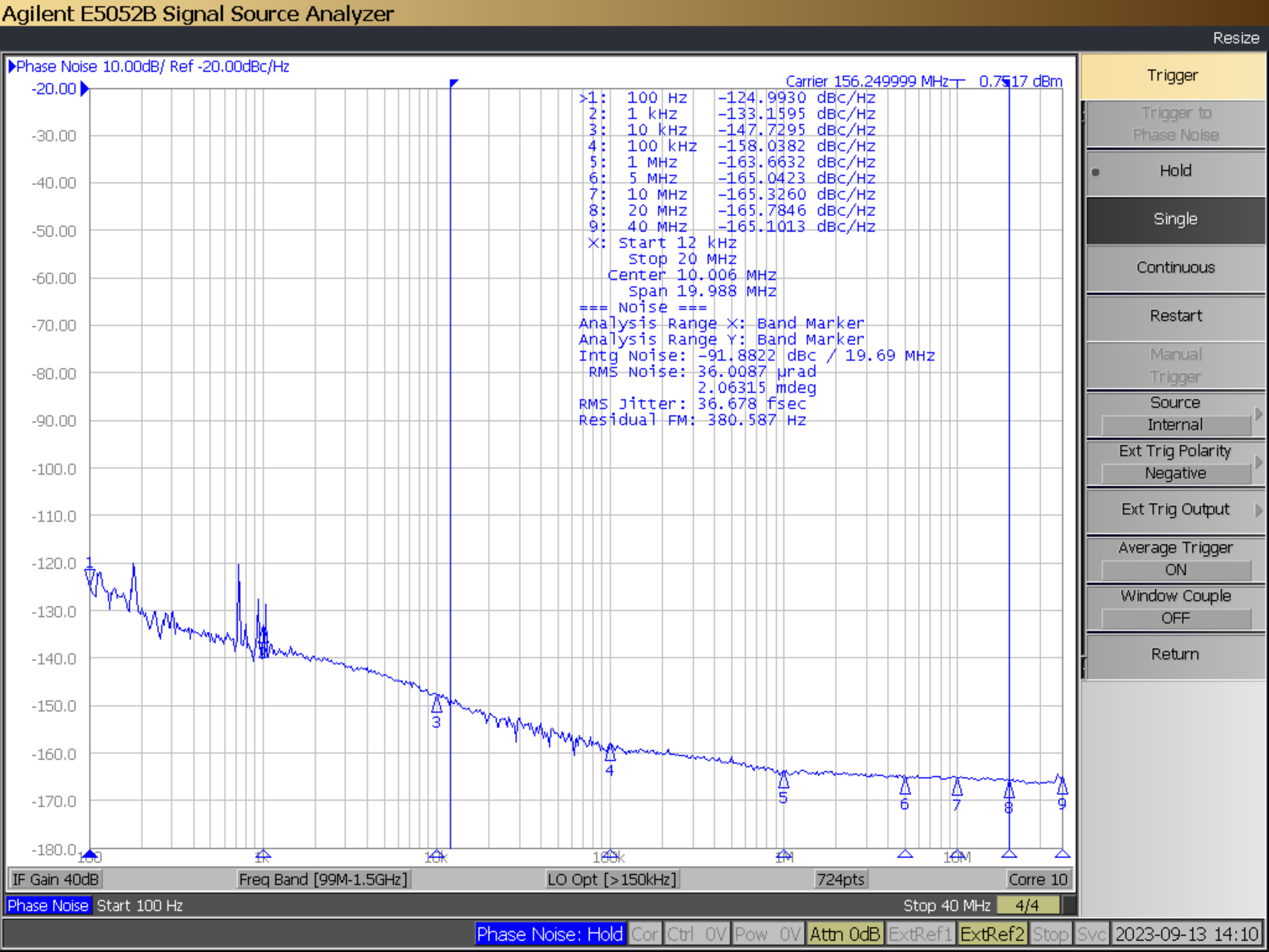
GUID-20231011-SS0I-NSZG-85LM-1VZHWBDMZNFX-low.png Figure 4-1 Reference Clock Input Phase Noise

GUID-20231011-SS0I-GC8F-403G-GVRCSBSRZK6S-low.svg

Figure 4-2 LMKDB1120 Output Clock Phase Noise