SNIS137G August 2004 – August 2019 LM95071
PRODUCTION DATA.
- 1 Features
- 2 Applications
- 3 Description
- 4 Revision History
- 5 Pin Configuration and Functions
-
6 Specifications
- 6.1 Absolute Maximum Ratings
- 6.2 ESD Ratings
- 6.3 Recommended Operating Ratings
- 6.4 Thermal Information
- 6.5 Temperature-to-Digital Converter Characteristics
- 6.6 Logic Electrical Characteristics - Digital DC Characteristics
- 6.7 Logic Electrical Characteristics - Serial Bus Digital Switching Characteristics
- 6.8 Timing Diagrams
- 6.9 Typical Characteristics
- 7 Parameter Measurement Information
- 8 Detailed Description
- 9 Device and Documentation Support
- 10Mechanical, Packaging, and Orderable Information
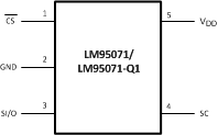
5 Pin Configuration and Functions
DBV Package
5-Pin SOT-23
Top View

Pin Function
| PIN | TYPE | DESCRIPTION | |
|---|---|---|---|
| NO. | NAME | ||
| 1 | CS | Input | Chip Select input. This pin receives an active-low signal from the controller to select the device. |
| 2 | GND | Ground | Ground. This is the power and signal ground return. |
| 3 | SI/O | Input/Output | Serial Input/Output. This serial, bidirectional, data bus pin transmits and receives signals to and from the controller. Schmitt trigger input in the input mode. |
| 4 | SC | Input | Serial bus clock. This serial clock signal comes from the controller. Schmitt trigger input. |
| 5 | VDD | Supply | Positive Supply Voltage. Supply a DC voltage from 2.4V to 5.5V to this pin and bypass with a 0.1-µF ceramic capacitor to ground. |