SNOA951 June 2016 LDC1312 , LDC1312-Q1 , LDC1314 , LDC1314-Q1 , LDC1612 , LDC1612-Q1 , LDC1614 , LDC1614-Q1
- Inductive Sensing Touch-On-Metal Buttons Design Guide
3.2.1 PCB Design
LDCs typically utilize a multi-layer PCB spiral inductor as the inductive element for the LC resonator circuit. An external capacitor is added in parallel to the sense coil as shown in Figure 2, whose value remains static regardless of metal proximity. The key coil parameters are shown in Figure 11.
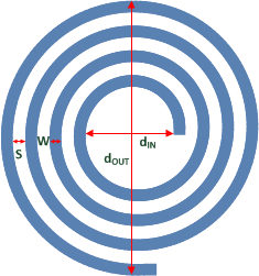 Figure 11. PCB Coil Parameters
 LDC sensor design guidelines are described in detail in the LDC Sensor Design application note (SNOA930).
When determining the geometries of the sensor coil for ToM applications, it is generally recommended to match the shape of coil to the metal button so that the deflection is evenly distributed over the sensor coil.
The outer diameter (dOUT) of the coil should be large enough to sense the metal proximity at the nominal distance, but due to the concave nature of a button press, very little metal is deflected at the edges of the metal button. Therefore it is recommended to keep the outer diameter between 50% to 60% of the metal button diameter to maximize the sensitive area of the coil to the metal deflection. Once the diameters of the metal button and the coil have been determined, the sensor PCB coil can be placed ideally within 20% of the coil diameter from the metal according to Figure 8. This nominal spacing can be achieved by using a spacer that is 20% of the coil diameter thick or by milling out the metal above the sensor.
The coil fill ratio is also important to consider for ToM applications, because the metal target deforms the most at the center when pressed and causes an uneven amount of coverage over the sensor coil with the closest proximity to the coil at the center. This deflection shape makes the inner turns more useful and therefore ToM sensors should use many inner turns as possible to achieve a dIN / dOUT ratio of less than 0.4. This effect can be seen by examining the eddy currents produced on the surface of the metal button. There is a higher density of eddy currents where the most magnetic field lines are concentrated as shown in Figure 12. Therefore by increasing the number of inner turns more eddy currents are generated on the surface of the metal which increases the sensitivity of the ToM system.
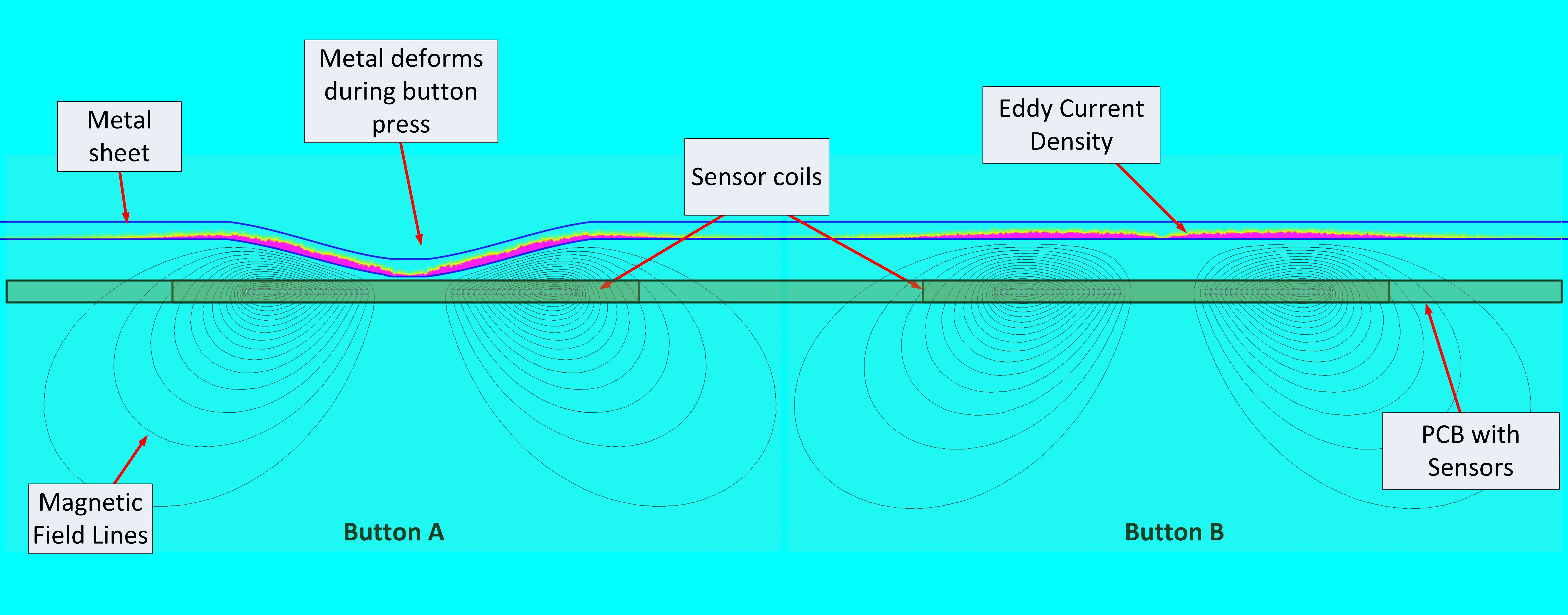 Figure 12. Eddy Current Density Induced by an AC Magnetic Field
 For this example application, a PCB with the coil characteristics in Table 1 was designed on a two-layer PCB, as shown in Figure 13 to Figure 15.
Table 1. Sensor Coil Parameters
| PARAMETER | VALUE |
|---|---|
| dOUT | 12 mm |
| dIN | 3.3 mm |
| Number of turns / layer | 14 |
| Number of layers | 2 |
| Trace width (W) | 6 mil (0.15 mm) |
| Trace spacing (S) | 6 mil (0.15 mm) |
With an inner metal surface-to-sensor distance of d1=0.55 mm, the coil design produces a nominal inductance of 3 µH. Note that although the metal button is 12 mm, the outer silkscreen with 20-mm diameter indicates the portion on the bottom of the metal panel which has been recessed by 0.55 mm to provide room for deflection of the button, refer to Figure 18.
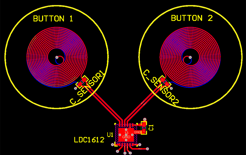 Figure 13. Sensor PCB (All Layers)
 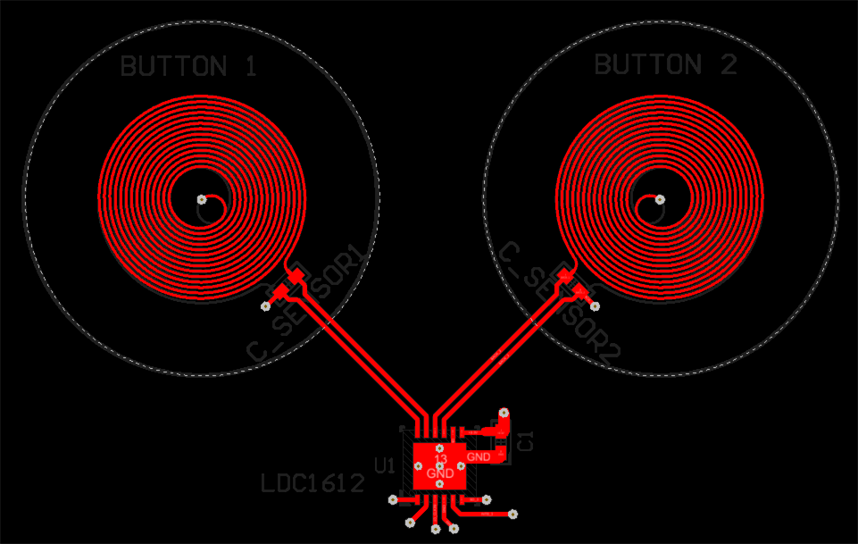 Figure 14. Sensor PCB (Top Layer)
 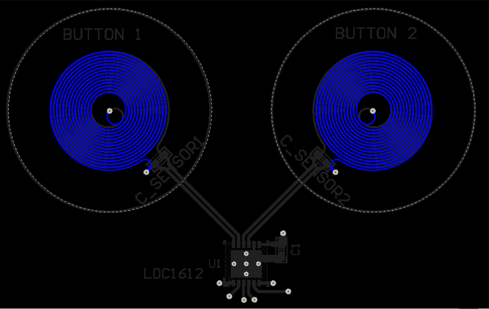 Figure 15. Sensor PCB (Bottom Layer)