SNOSCY4E March   2015  – October 2018 LMG5200

PRODUCTION DATA.  

  1. Features
  2. Applications
  3. Description
    1.     Device Images
      1.      Simplified Block Diagram
  4. Revision History
  5. Pin Configuration and Functions
    1.     Pin Functions
  6. Specifications
    1. 6.1 Absolute Maximum Ratings
    2. 6.2 ESD Ratings
    3. 6.3 Recommended Operating Conditions
    4. 6.4 Thermal Information
    5. 6.5 Electrical Characteristics
    6. 6.6 Typical Characteristics
  7. Parameter Measurement Information
    1. 7.1 Propagation Delay and Mismatch Measurement
  8. Detailed Description
    1. 8.1 Overview
    2. 8.2 Functional Block Diagram
    3. 8.3 Feature Description
      1. 8.3.1 Control Inputs
      2. 8.3.2 Start-up and UVLO
      3. 8.3.3 Bootstrap Supply Voltage Clamping
      4. 8.3.4 Level Shift
    4. 8.4 Device Functional Modes
  9. Application and Implementation
    1. 9.1 Application Information
    2. 9.2 Typical Application
      1. 9.2.1 Design Requirements
      2. 9.2.2 Detailed Design Procedure
        1. 9.2.2.1 VCC Bypass Capacitor
        2. 9.2.2.2 Bootstrap Capacitor
        3. 9.2.2.3 Power Dissipation
      3. 9.2.3 Application Curves
  10. 10Power Supply Recommendations
  11. 11Layout
    1. 11.1 Layout Guidelines
    2. 11.2 Layout Examples
  12. 12Device and Documentation Support
    1. 12.1 Device Support
      1. 12.1.1 Development Support
    2. 12.2 Documentation Support
      1. 12.2.1 Related Documentation
    3. 12.3 Receiving Notification of Documentation Updates
    4. 12.4 Community Resources
    5. 12.5 Trademarks
    6. 12.6 Electrostatic Discharge Caution
    7. 12.7 Glossary
  13. 13Mechanical, Packaging, and Orderable Information
    1. 13.1 Package Information

Typical Application

Figure 11 shows a synchronous buck converter application with VCC connected to a 5-V supply. It is critical to optimize the power loop (loop impedance from VIN capacitor to PGND). Having a high power loop inductance causes significant ringing in the SW node and also causes the associated power loss. Refer to the Layout Guidelines section for information on how to minimize this power loop.
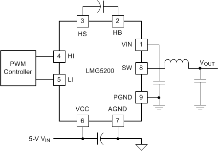
LMG5200 typ_app_1_snoscy4.gifFigure 11. Typical Connection Diagram For a Synchronous Buck Converter