SNOSDB8A June 2021 – December 2021 LM74701-Q1
PRODUCTION DATA
- 1 Features
- 2 Applications
- 3 Description
- 4 Revision History
- 5 Pin Configuration and Functions
- 6 Specifications
- 7 Parameter Measurement Information
- 8 Detailed Description
- 9 Application and Implementation
- 10Power Supply Recommendations
- 11Layout
- 12Device and Documentation Support
- 13Mechanical, Packaging, and Orderable Information
3 Description
The LM74701-Q1 is an automotive AEC Q100 qualified ideal diode controller which operates in conjunction with an external N-channel MOSFET as an ideal diode for low loss reverse polarity protection with a 20-mV forward voltage drop. LM74701-Q1 is suitable for input protection of 12-V automotive systems. The 3.2-V input voltage support is particularly well suited for severe cold crank requirements in automotive systems.
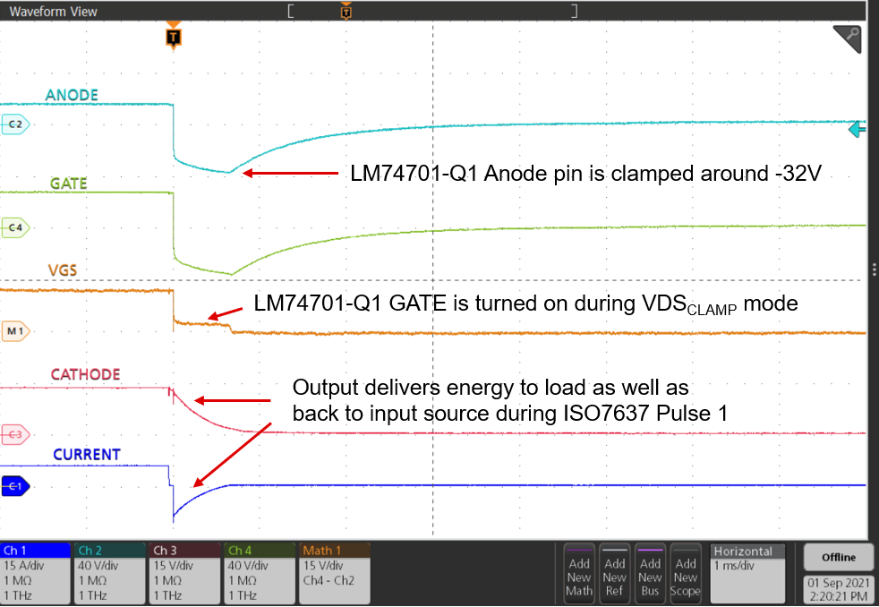
The device controls the GATE of the MOSFET to regulate the forward voltage drop at 20 mV. The regulation scheme enables graceful turn-off of the MOSFET during a reverse current event and ensures zero DC reverse current flow. Fast response (< 0.75 µs) to reverse current blocking makes the device suitable for systems with output voltage holdup requirements during ISO7637 pulse testing as well as power fail and input micro-short conditions. The LM74701-Q1 has a unique integrated VDS clamp feature which enables users to achieve TVS less input polarity protection solution and save on average a typical 60% of PCB space in constrained automotive systems.
The LM74701-Q1 controller provides a charge pump gate drive for an external N-channel MOSFET. With the enable pin low, the controller is off and draws approximately 1 µA of current.
| PART NUMBER | PACKAGE | BODY SIZE (NOM) |
|---|---|---|
| LM74701-Q1 | SOT-23 (8) | 2.90 mm × 1.60 mm |
 TVS Less ISO7637-2 Pulse 1 Performance