SNOU191 January   2022 LM74502-Q1 , LM74502H-Q1


  1.   Trademarks
  2. 1Introduction
    1. 1.1 Features
    2. 1.2 Applications
  3. 2Description
    1. 2.1 Input Power and Load (J1/J5 and J2/J6, J7/J11 and J8/J12)
    2. 2.2 Two Back-to-Back Connected MOSFETs (Q1/Q2–Q3/Q4 and Q6/Q7–Q8/Q9)
    3. 2.3 Output Slew Rate Control (R1 and C1)
    4. 2.4 Output Schottky Diode (D4, D10) and LED Indication (D6, D12)
    5. 2.5 Test Points
  4. 3Schematic
  5. 4Test Equipment Requirements
    1. 4.1 Power Supplies
    2. 4.2 Meters
    3. 4.3 Oscilloscope
    4. 4.4 Loads
  6. 5Test Setup and Results
    1. 5.1 Initial Setup
    2. 5.2 Power Up
    3. 5.3 Turn-ON with EN
    4. 5.4 Inrush Current Control
    5. 5.5 Overvoltage Response
    6. 5.6 Reverse Polarity Protection
  7. 6Board Layout and Bill of Materials
    1. 6.1 Board Layout
    2. 6.2 Bill of Materials

Test Setup and Results

This setup and results section describes the test procedure for the LM74502-Q1 device. A similar procedure applies for the LM74502H-Q1 device.

Table 5-1 shows the default jumper setting for LM74502Q1EVM board.

Table 5-1 Default Jumper Setting for LM74502Q1EVM
J4J3J10J9
1-2 for OV cutoff functionality1-2, output LED Indication1-2 for OV cutoff functionality1-2, output LED Indication
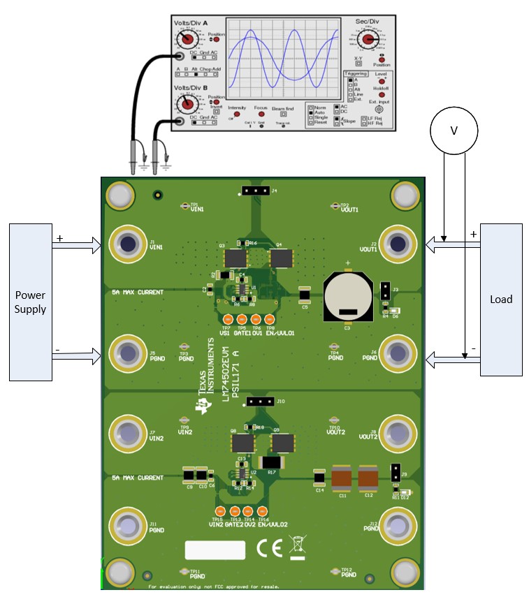
GUID-20211215-SS0I-HSQM-XZLZ-GL33G8KXWRBG-low.jpgFigure 5-1 LM74502Q1EVM Test Setup