SNVA067D April 2013 – August 2022 LM3478 , LM3481 , LM3488
5 Putting It Together
Now that the system has been modeled and the desired stability understood the compensation section can be designed. This is usually the last stage completed after the inductor and output capacitor selection. However, it might be prudent to revise these values if a better compensation scheme could be obtained. For instance, the output capacitor could be increased to bring in a pole to adjust the phase margin for improved settling on transient response.
To start selecting the compensation components it is good practice to have an idea where the crossover frequency should occur. With a boost converter like the LM3478 the right half plane zero causes severe difficulty with the loop response. Therefore, it is best to locate the crossover frequency one decade before this RHP zero occurs. If there is ever a choice between crossover frequencies it is best to choose the higher frequency.
Once the known equations have been calculated, the easiest way to set the compensation components is to use algebra on the graph technique for drawing bode plots. This allows the user to graphically place the pole and zero combinations to create the best response possible.
Design Example
To illustrate how to set the compensation for the LM3478 an example circuit will be used. Conditions:
Vin = 5V
Vout = 12V
Iload = 1.5A
Fs = 400KHz
Components:
L = 3.3uH
Cout = 150uF
ESR = 50mOhm
Calculations:
Duty-Cycle:
D' = 1 - D = 1 - 0.58 = 0.42
Control to Output Transfer Function
where:
Se = 3,320,000 A/Sec
Sn =1,515,151 A/Sec
Vout to Control Voltage:
AEA = gmROUT = 800µmho × 50kΩ = 38V/V
Therefore, the DC magnitude of the loop gain can be calculated:
ADC = AcompAcmAfb = 167 V/V × 38 V/V × 0.105 V/V = 665V/V
ADC = 20log10(665 V/V) = 56.4dB
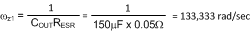
Since the RHP zero occurs at ~67KHz (420,875 rad/sec) the cross-over frequency should be set approximately a decade lower or ~6KHz. A point to remember is that this zero will decrease with heavier loads and lower input voltages. Therefore, a worst case condition would be with the minimum input voltage and maximum load. If a 10% tolerance was expected on the input rail this would mean we should set the cross-over frequency below 5KHz.
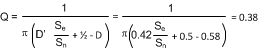
Using algebra on the graph we can now create our first bode plot without the compensation poles and zeroes. For simplicity Q was assumed to be equal to 0.5, which means that an identical real pole pair would be located at half the switching frequency. This is a reasonable first pass approximation given that the value for Q was found to be 0.38
 Figure 5-1 Uncompensated Loop
Gain
Figure 5-1 Uncompensated Loop
GainThe next step is to calculate the exact placement of the compensation pole and zero to get the desired response. First, we will decide on the pole placement to get the crossover frequency desired before using the zero to obtain the phase margin. Typically this process can undergo multiple revisions, including the power components.
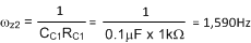
Knowing that we want a cross-over frequency below 5KHz we can observe that the magnitude in the range of 1KHz - 5KHz is 25dB to 35dB. To ensure adequate roll-off the compensation pole was chosen to be ~30Hz which is 2 decades back from the middle of the range. This also correspondeds to a capacitor of 0.1uF that is a commonly available size.
Updating the bode it can be seen that the magnitude is well below unity before the RHP zero occurs.
 Figure 5-2 Loop Gain with Dominant
Componsation Pole
Figure 5-2 Loop Gain with Dominant
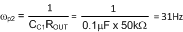
Componsation PoleThe last component necessary is the compensation resistor which sets a zero in the loop gain. It will be necessary to introduce this zero in the proximity of the cross-over frequency (~1KHz), because looking at the second bode plot the phase margin will be close to zero. This is because 2 poles have already occurred a decade before which introduces a phase change of 180 degrees. Therefore a zero in this location would correspond to approximately 45 degrees of phase margin. The bandwidth can also be increased safely as the gain is lower than –40dB before the next zero is introduced. Choosing a value of 1000 Ohms:
Now that the values have been obtained a full bode plot generated from the derived equation can be plotted and modifications made if necessary. As can be seen, the crossover frequency is 2KHz with a phase margin of 60 degrees.
 Figure 5-3 Loop Gain
Magnitude
Figure 5-3 Loop Gain
Magnitude Figure 5-4 Phase Margin of Loop
Gain
Figure 5-4 Phase Margin of Loop
GainOverall this method represents a simple analysis that can be performed to design an effective compensation network. It should be remembered that variations in all the components will occur, therefore bench analysis should always be used to verify stability.