SNVA067D April 2013 – August 2022 LM3478 , LM3481 , LM3488
1 Overview
The first question that is often asked is: Why is compensation necessary? Any DC-DC converter that regulates the output voltage utilizes negative feedback to ensure accuracy across line and load changes. An incorrect compensation scheme could lead to a phase reversal of the loop causing positive feedback and an erratic uncontrolled output. A minor problem that is typically encountered is an over or under-damped response of the output when a load transient is experienced. This is a sign that the loop stability could be optimized.
Before compensation components can be selected and the response measured, the first step to undertake is to understand the operation of the controller and feedback loops. It is assumed that you are already familiar with the basic operation of the switcher covered in LM3478 High-Efficiency Low-Side N-Channel Controller for Switching Regulator. Examining the block diagram of the LM3478 boost regulator in Figure 1-1, it can be clearly seen that two feedback loops exist. This is a unique feature that is indicative of a current mode control switching regulator.
The first loop is the output voltage loop created by VOUT passing through the resistor divider into an error amplifier. The output of the error amplifier is referred to as the control voltage, VC, which is one of the two inputs to the PWM comparator.
The other input to the comparator is the second feedback loop. With current mode control architecture the switch current is sensed and is used to determine, in conjunction with the control voltage, when the FET should be turned off. To achieve this the switch current is measured across the external sense resistor before being summed with an internal ramp. The slope compensation ramp is present to prevent a large signal stability issue that is inherent in current mode control. While this ramp voltage is included in our small signal models, its requirement and adjustment will not be discussed here. For more information about the slope compensation, please consult the LM3478 data sheet.
Figure 1-1 shows the overall block diagram of the LM3478 with its application circuit. The next step is to derive the small signal equation for the entire loop. To simplify the analysis the loop can be effectively divided into three separate parts. The first transfer function that will be examined is the control voltage, VC, to the output voltage, VOUT. This takes into account the effects of the current loop, switch, and the output filter stage such as the inductor and output capacitor.
 Figure 1-1 Overview of LM3478 Current Mode
Control Boost Regulator
Figure 1-1 Overview of LM3478 Current Mode
Control Boost RegulatorThe equation can be written as:
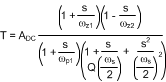
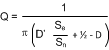
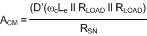
At first inspection the equation consists of two zeros, one of which is in the right half plane, a single pole and a complex pole pair. The DC gain of the system is written ACM and can be calculated by the equation:
where

and

and

and

This is a rather long formula that incorporates the slope compensation and the inductor into the equation. It has been provided for completeness, however in this analysis the equation has been reduced to a simpler and more manageable form. You will find this simplification works extremely well and no real noticeable difference will be seen in the analysis. Therefore for all LM3478 compensation calculations this equation should be used:

The next step is to calculate the two zeros that were found in the control to output equation. The first zero is created by the output capacitor and its associated equivalent series resistance:

The second zero is actually a right half plane zero. When examining its response on a bode plot it has the effect of increasing the gain by 20dB/decade like a left hand plane zero, but causing a 90 degree drop in phase like a pole. Its occurrence can be related to the application circuit by thinking of the response of the output voltage. If the output voltage starts dropping the switch will turn on to increase the current through the inductor. This causes the output voltage to drop even lower since the output current is provided solely by the output capacitor during this time. It is this effect that can be thought of as the source of the right half plane zero, which explains why it does not occur in a buck converter.
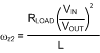
Looking at the denominator of the equation the poles can be calculated. The first pole is from the output capacitor and the load resistance and can be expressed as:
The complex pole pair occurs at half the switching frequency and will be simply attributed to sampling theory for the sake of length in this application note. A Q factor also appears that can be calculated based on the inductor current slopes and duty-cycle:
ωs = 2 x π x fs