SNVA432D March 2010 – January 2022 LM21305
9.3 Switching Frequency Selection
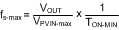
The LM21305 supports a wide range of switching frequencies: 300 kHz to 1.5 MHz. The choice of switching frequency is usually a compromise between efficiency and size of the circuit. Lower switching frequency usually implies lower switching losses (including gate charge losses, transition losses, etc.) and would typically result in a better efficiency. But higher switching frequency allows the use of smaller LC filters to achieve a more compact design. Lower inductance also helps transient response (faster large-signal slew rate of inductor current) and reduces the conduction loss associated with the inductor DCR. The optimal switching frequency for efficiency needs to be determined on a case by case basis. It is related to the input voltage, the output voltage, the most frequent load level, external component choices, and circuit size requirement. The choice of switching frequency is also limited if an operating condition is possible to trigger TON-MIN and TOFF-MIN. The maximum frequency that can be used for a given input and output voltage can be found by:
The following equation should be used to calculate resistor R4 value in order to obtain a desired frequency of operation:
fs [kHz] = 31000 × R−0.9[kΩ]