SNVA432D March 2010 – January 2022 LM21305
9.6 Compensation Circuit
The LM21305 is designed to achieve high performance in terms of the transient response, audio susceptibility and output impedance, and will typically require only a single resistor Rc and capacitor Cc1 for compensation. However, depending on the power stage, it could require a second capacitor to create a high frequency pole to cancel the output capacitor ESR.
 Figure 9-1 LM21305 Compensation Network
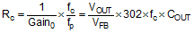
To select the compensation components, a desired cross over frequency fc should be selected first. It is recommended to select fc equal to or lower than fs/6. A simplified procedure is given below for Rc and Cc1, assuming the capacitor ESR zero is at least three times higher than fc. The compensation resistor can be found by:
Cc1 does not affect the crossover frequency fc, but it sets the compensator zero fZcomp and affects the phase margin of the loop. For a fast design, Cc1 = 4.7 nF gives adequate performance in most LM21305 applications. Larger Cc1 capacitance gives higher phase margin but at the expese of longer transient response settling time. It is recommended to set the compensation zero no higher than fc/3 to ensure enough phase margin, implying:

For more details, see the LM21305 5A Adjustable Frequency Synchronous Buck Regulator Data Sheet (SNVS639).