SNVA912A January 2020 – April 2021 REF34-Q1
4.2 DBV-5 Package
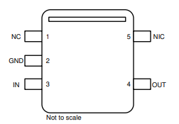
Figure 4-2 shows the REF34-Q1 pin diagram for the DBV-5 package. For a detailed description of the device pins please refer to the Pin Configuration and Functions section in the REF34-Q1 data sheet.
 Figure 4-2 Pin Diagram (DBV-5 Package)
Table 4-6 Pin FMA for Device Pins
Short-Circuited to Ground
| Pin Name | Pin No. | Description of Potential Failure Effect(s) | Failure Effect Class |
|---|---|---|---|
| NC | 1 | No effect | D |
| GND | 2 | No effect | D |
| IN | 3 | No output voltage, high leakage | B |
| OUT | 4 | No output voltage | B |
| NC | 5 | No effect | D |
Table 4-7 Pin FMA for Device Pins
Open-Circuited
| Pin Name | Pin No. | Description of Potential Failure Effect(s) | Failure Effect Class |
|---|---|---|---|
| NC | 1 | No effect | D |
| GND | 2 | No output voltage | D |
| IN | 3 | Output is not regulated | C |
| OUT | 4 | Output is not regulated | C |
| NC | 5 | No effect | D |
Table 4-8 Pin FMA for Device Pins
Short-Circuited to Adjacent Pin
| Pin Name | Pin No. | Shorted to | Description of Potential Failure Effect(s) | Failure Effect Class |
|---|---|---|---|---|
| NC | 1 | GND | No effect | D |
| GND | 2 | IN | Disables device, no output, high leakage | B |
| IN | 3 | OUT | Output not regulated, high leakage | B |
| OUT | 4 | NC | No effect | D |
| NC | 5 | NC | No effect | D |
Table 4-9 Pin FMA for Device Pins Short-Circuited to
Supply
| Pin Name | Pin No. | Description of Potential Failure Effect(s) | Failure Effect Class |
|---|---|---|---|
| NC | 1 | No effect | D |
| GND | 2 | No output voltage, high leakage | B |
| IN | 3 | No effect | D |
| OUT | 4 | Output is not regulated | C |
| NC | 5 | No effect | D |