SNVAA71 October 2023 TPSM63610
2.2 Start-up Behavior and Switching Node Consideration
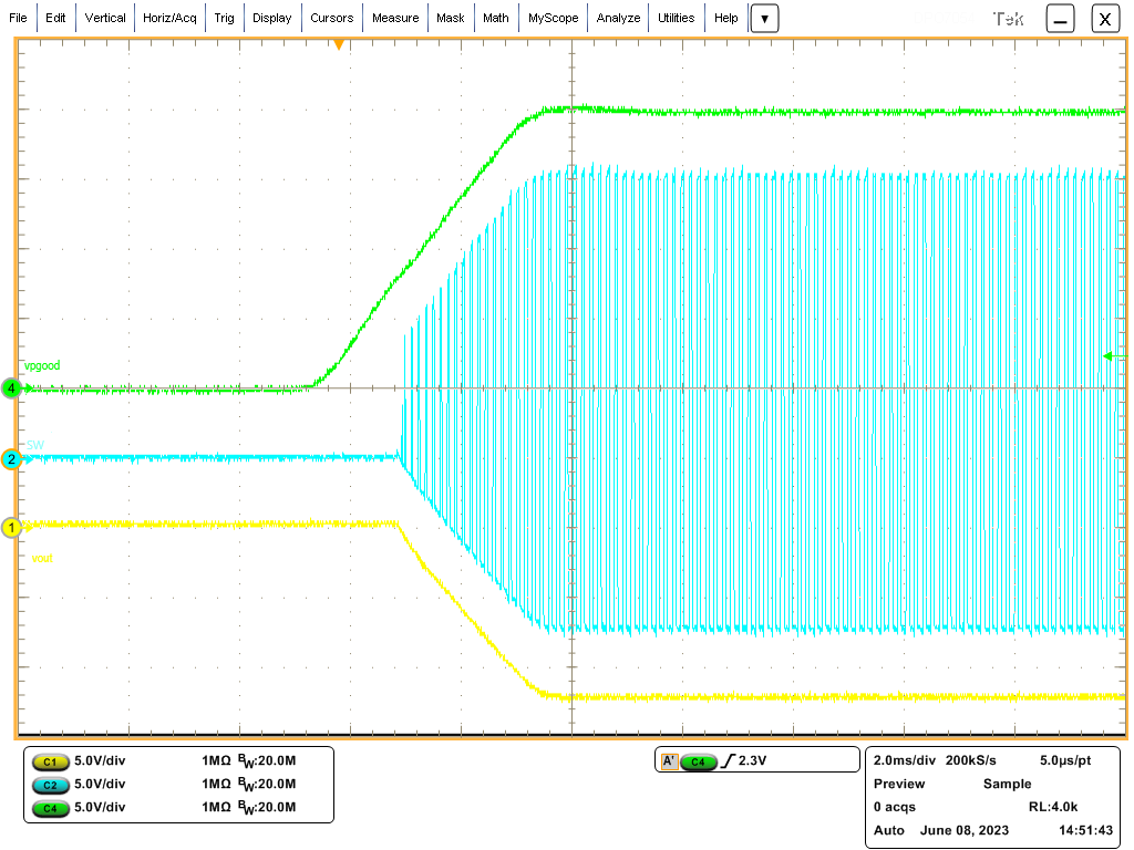
The voltage on the SW pin switches from VIN to VOUT in an inverting topology instead of from VIN to GND in a buck topology. When the high-side MOSFET turns on, the SW node is pulled up to the input voltage. When the low-side MOSFET turns on, the SW node is pulled to -VOUT. The output voltage starts to go negative after the EN pin voltage exceeds its threshold level and VIN exceeds its UVLO threshold. As VOUT continues to go negative, the SW node tracks the negative output voltage. Figure 2-2 shows the resulting normal and smooth start-up of the output voltage.
 Figure 2-2 Typical SW Node
Characteristics During Start-Up