SNVAA76 june 2023 TPS7H4010-SEP
2 Detailed Design Procedure
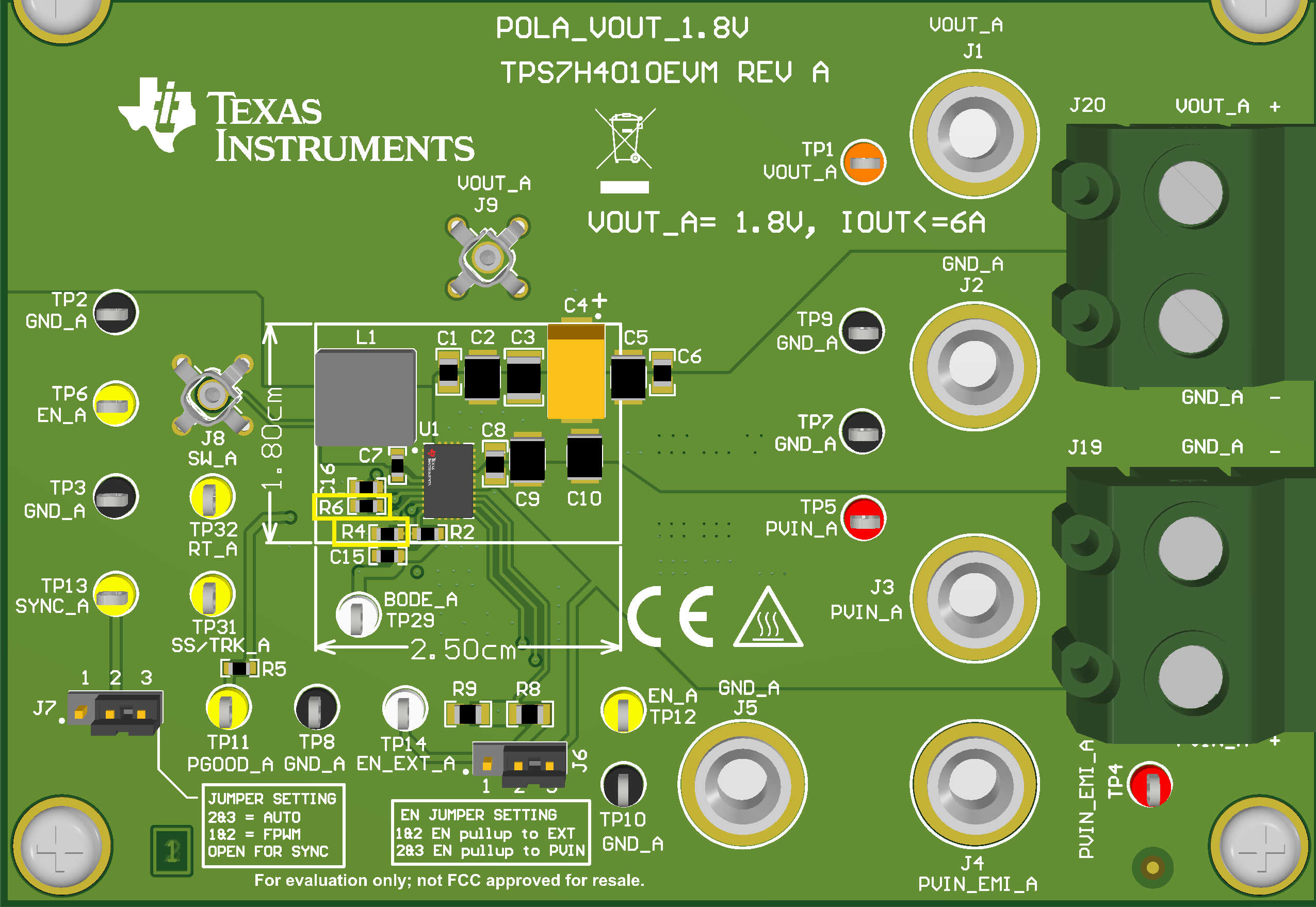
For this application note, the inverting buck-boost is implemented using the TPS7H4010EVM. The TPS7H4010EVM has two TPS7H4010-SEP devices on the board. One device is configured to output 3.3V and the other is configured to output 1.8V. The following instructions on how to configure the TPS7H4010EVM in an inverting buck-boost topology is referred to the 1.8 V rail on the EVM (Figure 2-1). The first step is to ground the output labeled as VOUT_A (TP1, J1, top of J20) on the board. Then for the output and load, connect that to the EVM ground labeled GND_A (TP9, J2, bottom of J20). The input voltage is still connected across PVIN_A (TP5, J3) and VOUT_A (TP1, J1, top of J20) since this is what the ground is tied to. This process configures the EVM into the inverting buck-boost configuration.
| Vout | L1 (L3) (uH) | Cout | R2(R12) (Ω) | R4(R14)(Ω) | R6(R16)(Ω) |
|---|---|---|---|---|---|
| -12 V | 3.3 uH | 141 uF | 100 k | 9.1 k | 39.2 k |
| -6 V | 3.3 uH | 141 uF | 100 k | 20 k | 39.2 k |
| -1.8 V | 1.8 uH | 400 uF | 100 k | 124 k | 39.2 k |
The design considerations for each of the different rails tested is discussed. For the TPS7H4010-SEP inverting buck-boost topology, a switching frequency of 1 MHz was set. For these changes to be made on the TPS7H4010EVM, some passive component values were changed on what was originally the 3.3 V rail to convert to the -12 V and -6 V rails and on the original 1.8 V to convert to -1.8 V. To do this, first on both the 3.3 V rail and the 1.8 V rail of the EVM R16 (R6 on the 1.8-V rail) was replaced with a 39.2-k resistor to change the switching frequency to the desired 1-MHz switching frequency. Then to change the output voltage value of the 3.3 V rail, the feedback resistor R14 was changed to regulate to -12 V and -6 V. Table 2-1 shows the passive values used for the design of each of the output rails tested for the inverting buck-boost application. The table includes two numbers for each of the passive values corresponding to the number on the schematic based on the initial 1.8 V rail (3.3 V rail) schematic. Both resistors that need to be changed are highlighted in Figure 2-1 of the TPS7H4010EVM. The remainder of the passive values have stayed the same for the testing performed. Note that other passive values can be changed to optimize for the specific output regulation required.
 Figure 2-1 TPS7H4010EVM 3.3-V Layout