SNVAA76 june 2023 TPS7H4010-SEP
1.1 Design Description
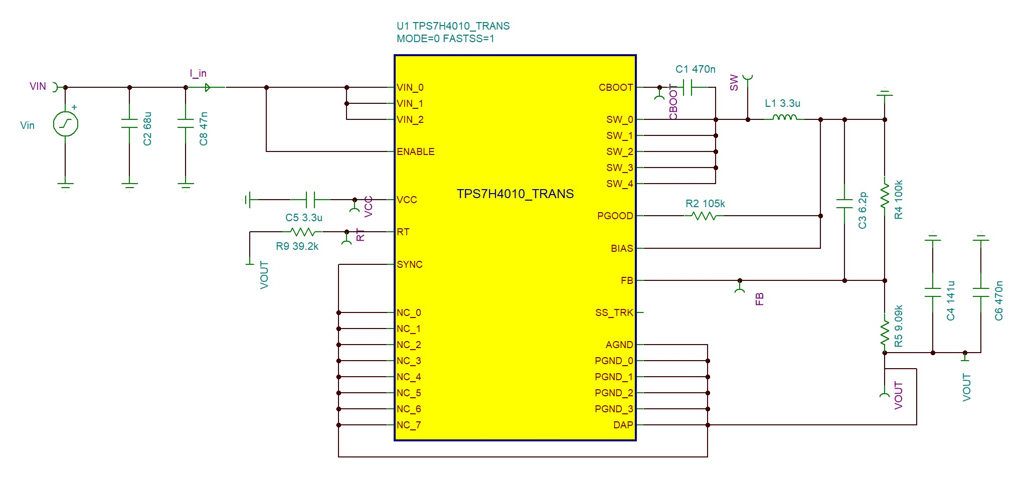
Implementing the TPS7H4010-SEP as an inverting buck-boost is similar to buck topology. In the buck topology, the positive connection of the output is connected to the inductor and the return is connected to the integrated circuit (IC) ground. In the inverting buck-boost configuration however, the IC ground is used as the negative output voltage and what used to be the positive output is connected to ground. The inverting buck-boost topology allows the output voltage to be inverted and lower than ground because Vin is typically referred to ground, but in the inverting buck-boost topology, Vin is referred to Vout. The input voltage range of the TPS7H4010-SEP in the inverting buck-boost is 3.5-V to 32-V (+ Vout), where Vout is a negative value. Since the input is switching from Vin all the way to Vout instead of ground, remember to pick adequately rated capacitors for the input. The maximum output current is reduced when going from buck to inverting buck-boost configuration. For this application, 3 A was the maximum current tested as exceeding 3 A is not recommended. Figure 1-1 shows the schematic for the inverting buck-boost topology.
 Figure 1-1 TPS7H4010-SEP Inverting Buck Boost Topology