SNVSB48C April 2018 – October 2019 LMR36006
PRODUCTION DATA.
- 1 Features
- 2 Applications
- 3 Description
- 4 Revision History
- 5 Device Comparison Table
- 6 Pin Configuration and Functions
- 7 Specifications
- 8 Detailed Description
-
9 Application and Implementation
- 9.1 Application Information
- 9.2
Typical Application
- 9.2.1
Design 1: Low Power 24-V, 600-mA PFM Converter
- 9.2.1.1 Design Requirements
- 9.2.1.2
Detailed Design Procedure
- 9.2.1.2.1 Custom Design With WEBENCH Tools
- 9.2.1.2.2 Choosing the Switching Frequency
- 9.2.1.2.3 Setting the Output Voltage
- 9.2.1.2.4 Inductor Selection
- 9.2.1.2.5 Output Capacitor Selection
- 9.2.1.2.6 Input Capacitor Selection
- 9.2.1.2.7 CBOOT
- 9.2.1.2.8 VCC
- 9.2.1.2.9 CFF Selection
- 9.2.1.2.10 Maximum Ambient Temperature
- 9.2.2 Application Curves
- 9.2.3 Design 2: High Density 24-V, 600-mA PFM Converter
- 9.2.1
Design 1: Low Power 24-V, 600-mA PFM Converter
- 9.3 What to Do and What Not to Do
- 10Power Supply Recommendations
- 11Layout
- 12Device and Documentation Support
- 13Mechanical, Packaging, and Orderable Information
8.3.3 Current Limit and Short Circuit
The LMR36006 incorporates valley current limit for normal overloads and for short-circuit protection. In addition the high-side power MOSFET is protected from excessive current by a peak current limit circuit. Cycle-by-cycle current limit is used for overloads, while hiccup mode is used for short circuits. Finally, a zero current detector is used on the low-side power MOSFET to implement diode emulation mode (DEM) at light loads (see Glossary).
During overloads the low-side current limit, ILIMIT, determines the maximum load current that the LMR36006 can supply. When the low-side switch turns on, the inductor current begins to ramp down. If the current does not fall below ILIMIT before the next turnon cycle, then that cycle is skipped, and the low-side MOSFET is left on until the current falls below ILIMIT. This is somewhat different than the more typical peak current limit and results in Equation 1 for the maximum load current.

where
- fSW = switching frequency
- L = inductor value
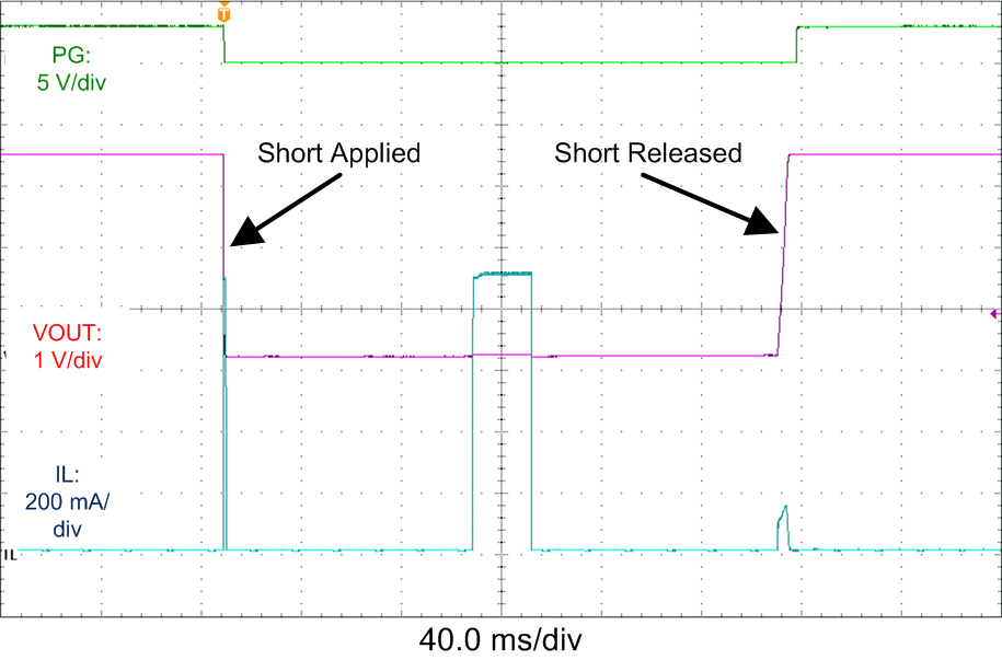
If, during current limit, the voltage on the FB input falls below about 0.4 V due to a short circuit, the device enters into hiccup mode. In this mode the device stops switching for tHC or about 94 ms, and then goes through a normal re-start with soft start. If the short-circuit condition remains, the device runs in current limit for about 20 ms (typical) and then shuts down again. This cycle repeats, as shown in Figure 12 as long as the short-circuit condition persists. This mode of operation helps to reduce the temperature rise of the device during a hard short on the output. Of course the output current is greatly reduced during hiccup mode. Once the output short is removed and the hiccup delay is passed, the output voltage recovers normally as shown in Figure 12.
The high-side-current limit trips when the peak inductor current reaches ISC. This is a cycle-by-cycle current limit and does not produce any frequency or load current fold back. It is meant to protect the high-side MOSFET from excessive current. Under some conditions, such as high input voltages, this current limit may trip before the low-side protection. Under this condition, ISC determines the maximum output current. Note that ISC varies with duty cycle.
 Figure 12. Short-Circuit Transient and Recovery