SNVSB48C April 2018 – October 2019 LMR36006
PRODUCTION DATA.
- 1 Features
- 2 Applications
- 3 Description
- 4 Revision History
- 5 Device Comparison Table
- 6 Pin Configuration and Functions
- 7 Specifications
- 8 Detailed Description
-
9 Application and Implementation
- 9.1 Application Information
- 9.2
Typical Application
- 9.2.1
Design 1: Low Power 24-V, 600-mA PFM Converter
- 9.2.1.1 Design Requirements
- 9.2.1.2
Detailed Design Procedure
- 9.2.1.2.1 Custom Design With WEBENCH Tools
- 9.2.1.2.2 Choosing the Switching Frequency
- 9.2.1.2.3 Setting the Output Voltage
- 9.2.1.2.4 Inductor Selection
- 9.2.1.2.5 Output Capacitor Selection
- 9.2.1.2.6 Input Capacitor Selection
- 9.2.1.2.7 CBOOT
- 9.2.1.2.8 VCC
- 9.2.1.2.9 CFF Selection
- 9.2.1.2.10 Maximum Ambient Temperature
- 9.2.2 Application Curves
- 9.2.3 Design 2: High Density 24-V, 600-mA PFM Converter
- 9.2.1
Design 1: Low Power 24-V, 600-mA PFM Converter
- 9.3 What to Do and What Not to Do
- 10Power Supply Recommendations
- 11Layout
- 12Device and Documentation Support
- 13Mechanical, Packaging, and Orderable Information
8.4.3 Minimum Switch On-Time
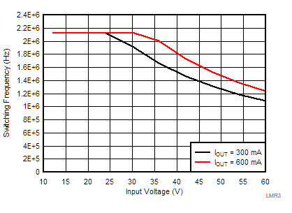
Every switching regulator has a minimum controllable on-time dictated by the inherent delays and blanking times associated with the control circuits. This imposes a minimum switch duty cycle and therefore a minimum conversion ratio. The constraint is encountered at high input voltages and low output voltages. To help extend the minimum controllable duty cycle, the LMR36006 automatically reduces the switching frequency when the minimum on-time limit is reached. In this way the converter can regulate the lowest programmable output voltage at the maximum input voltage. An estimate for the approximate input voltage, for a given output voltage, before frequency foldback occurs is found in Equation 2. As the input voltage is increased, the switch on-time (duty cycle) reduces to regulate the output voltage. When the on-time reaches the limit, the switching frequency drops, while the on-time remains fixed.

 Figure 17. Switching Frequency vs Input Voltage
VOUT = 3.3 V