SNVU658B March 2020 – May 2021
- Trademarks
- 1Introduction
-
2Test Setup and Results
- 2.1 Input/Output Connections
- 2.2 Start Up Procedure
- 2.3 Efficiency
- 2.4 Load and Line Regulation
- 2.5 Load Transients
- 2.6 Loop Characteristics
- 2.7 Output Voltage Ripple
- 2.8 Input Voltage Ripple
- 2.9 Powering Up and Down with EN
- 2.10 Powering Up and Down With VIN
- 2.11 Start-Up Into Pre-Bias
- 2.12 Current Limit
- 3Schematic, List of Materials, and Layout
- Revision History
1.3.1 Output Voltage Setpoint
The output voltage is set by a resistor divider network of R3 and R7. Keeping R7 fixed and change the output voltage of the EVM by changing the value of resistor R3. Changing the value of R3 will change the output voltage above the reference voltage VINTREF.
The value of R3 for a specific output voltage can be calculated using Equation 1
Equation 1. 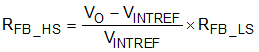
VINTREF= 0.9 V for TPS54J060
VINTREF= 0.6 V for TPS54J061
RFB_HS = R3
RFB_LS = R7