SNVU682A July 2019 – March 2021 LM61495-Q1
5 Board Layout
Figure 5-1 through Figure 5-6 show the board layout for the LM61495RPHEVM. The EVM offers resistors, capacitors, and jumpers to configure the output voltage and precision enable pin, and set frequency and external clock synchronization among the other features of the LM61495-Q1.
The PCB is optimized for thermal performance. The board contains 4 layers. There are 2-oz copper layers on the top and bottom and 1-oz copper mid-layers. The LM61495-Q1 does not have a thermal pad so the best path to move the heat out of the IC is through the pins and into the board. The PGND pins connect to the large GND plane which spreads the heat to the rest of the board. The GND plane also has thermal vias to spread the heat more efficiently to other layers for additional improved thermal performance.
The PCB is also optimized for EMI performance. The layout minimizes the area of high dv/dt nodes like SW and BOOT. The small high-frequency ceramic input capacitors are placed very close to the IC to minimize the loop formed from VIN pins, through the capacitor, to the PGND pins. The board also features an EMI filter on the back-side of the board with options for an inductor, ferrite bead, and filter capacitors to tune the desired EMI performance. The full filter may not be necessary to pass particular EMI requirements but the components and pads are available for flexibility in adjustments.
The screw terminals J1 and J2 allow for high-current connections to the board. Jumper J3 connects VOUT to BIAS for improved light-load efficiency. Jumper J4 allows the user to select the output voltage, 5V or 3.3V. J5 allows the user to turn on or off Spread Spectrum. J6 allows the user to operate the device in AUTO mode (pulse frequency modulation at light loads) or FPWM (forced pulse width modulation). The MODE/SYNC pin on J6 also acts as a SYNC pin to synchronize to an external clock if desired. J7 allows the user to enable or disable the IC.
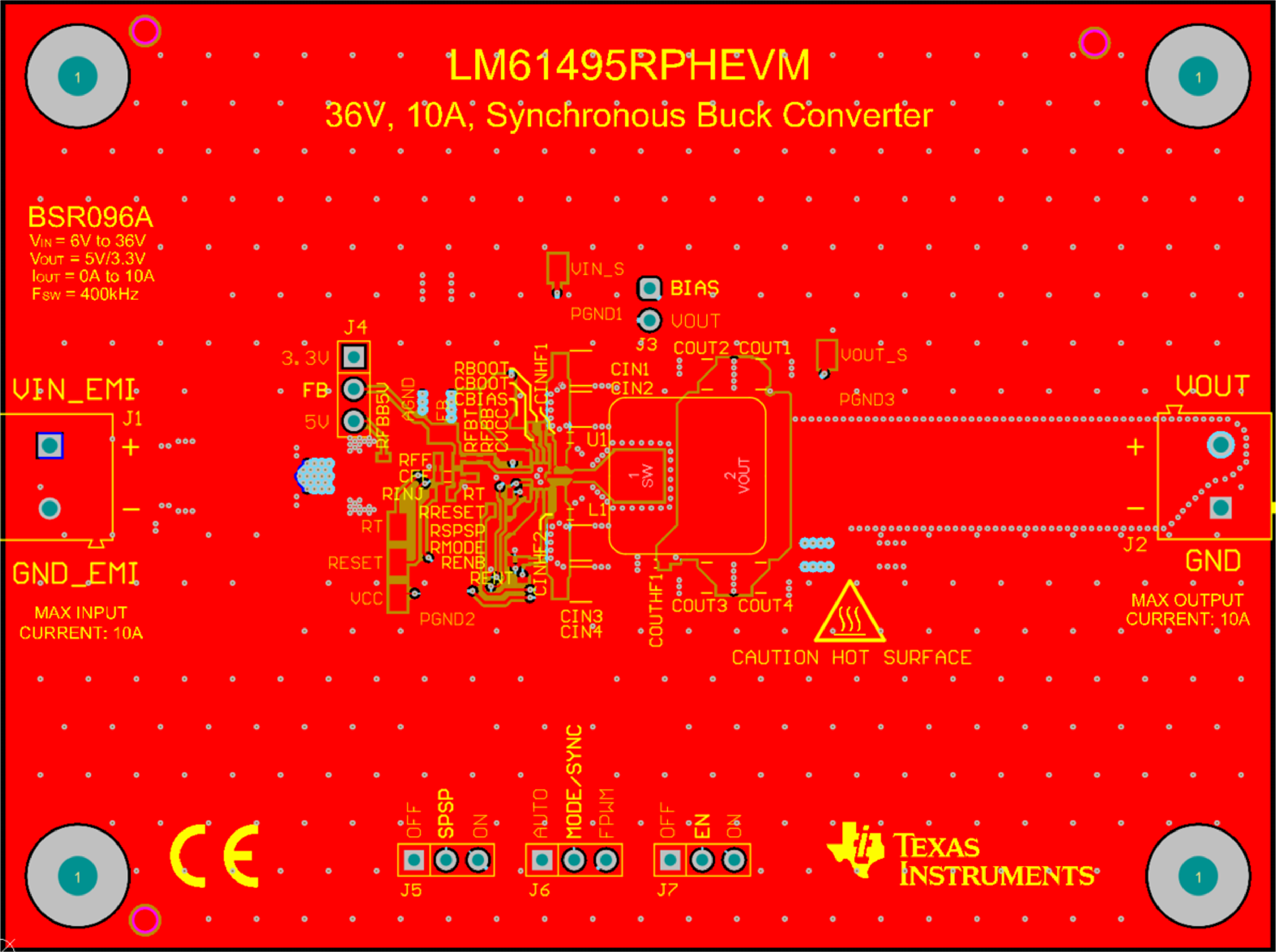 Figure 5-1 Top layer and top silkscreen
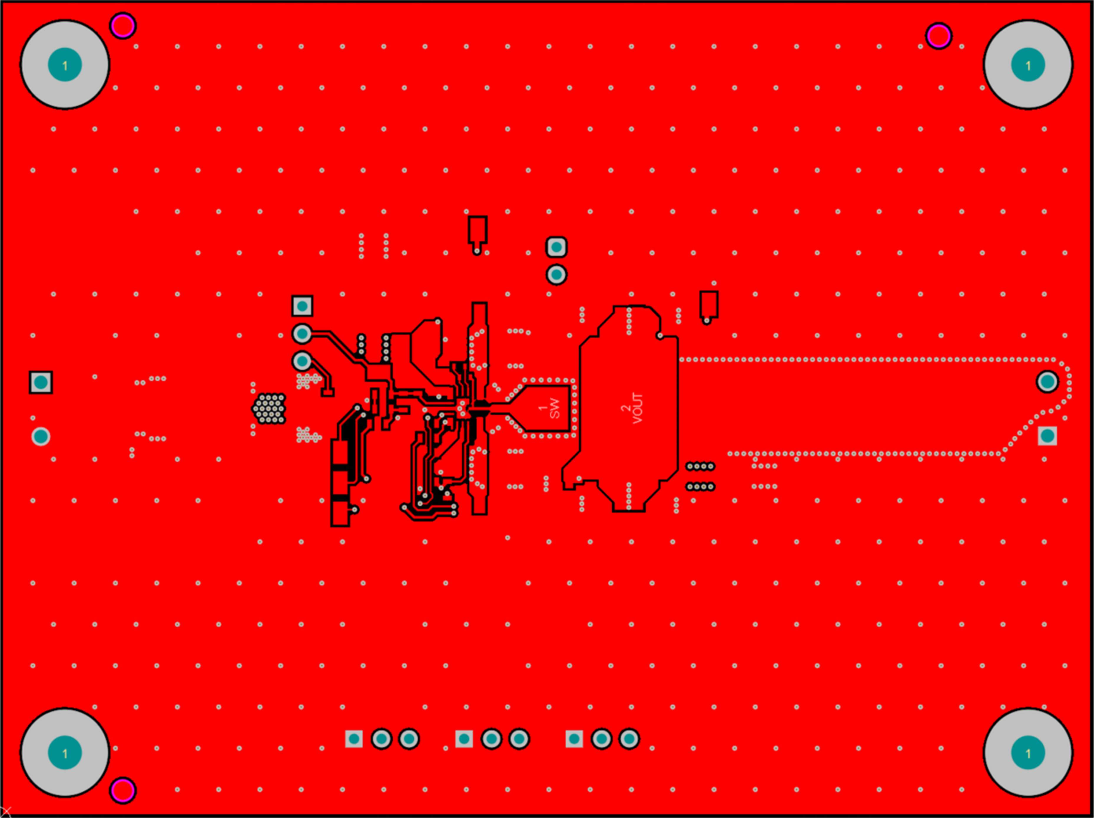 Figure 5-2 Top layer routing
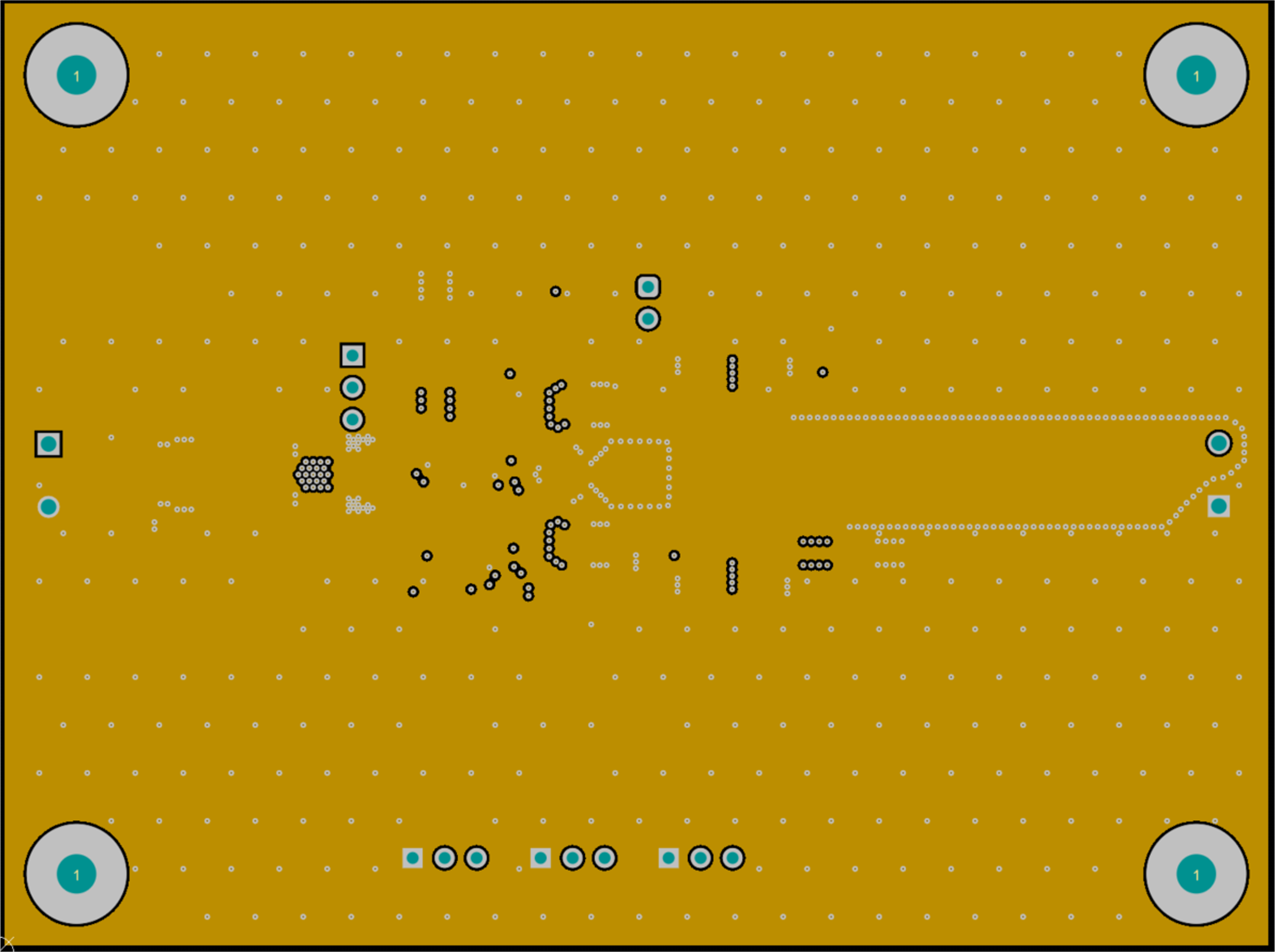 Figure 5-3 Mid-layer 1 ground plane
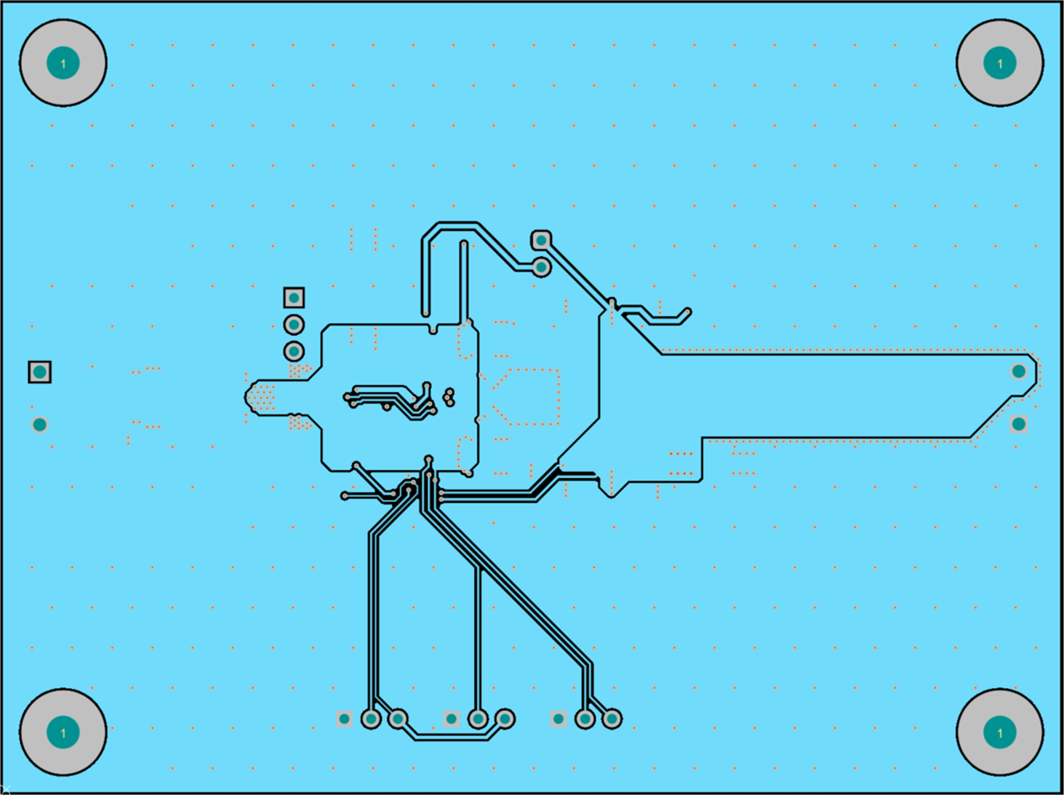 Figure 5-4 Mid-layer 2 routing
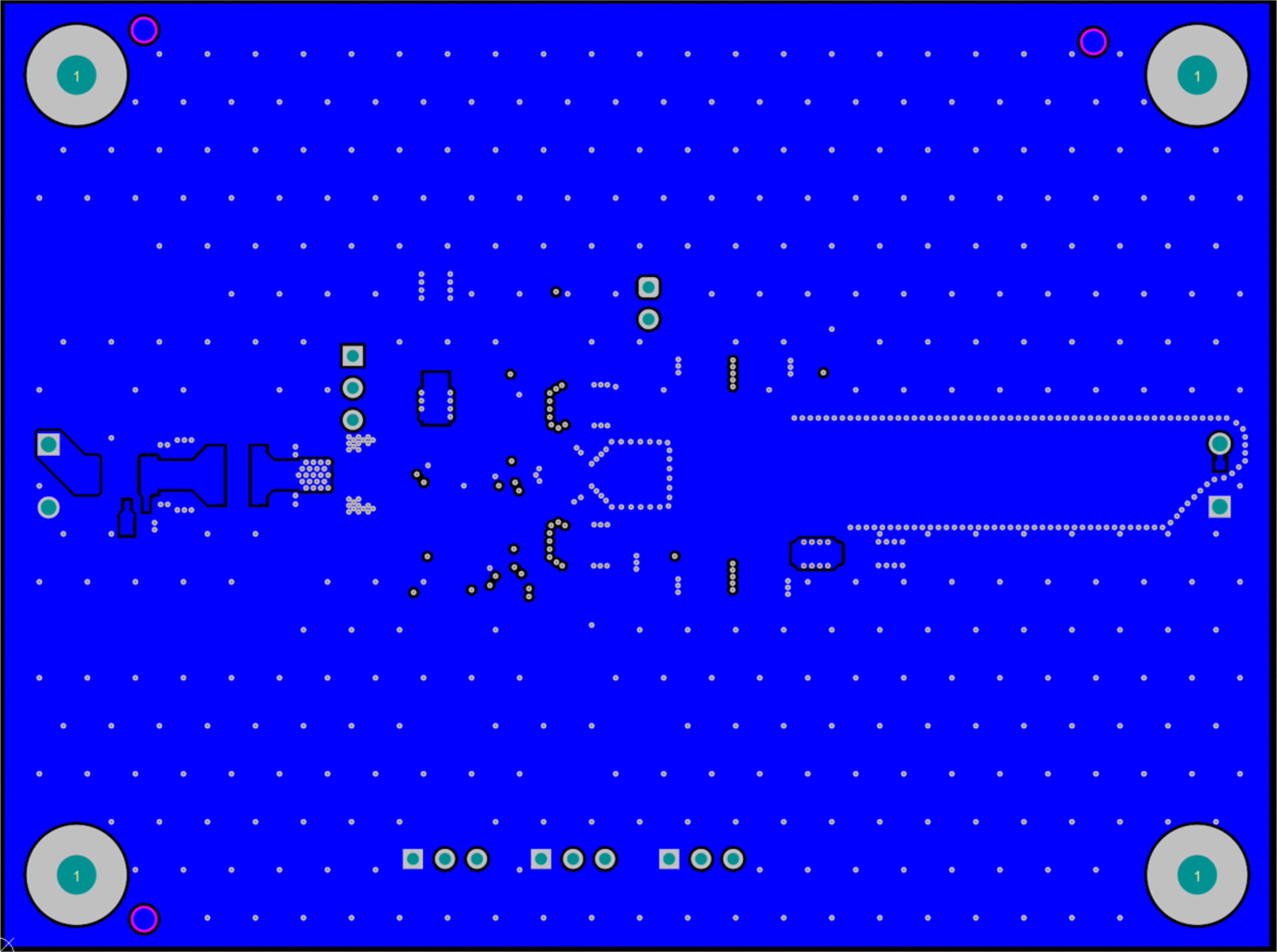 Figure 5-5 Bottom layer routing
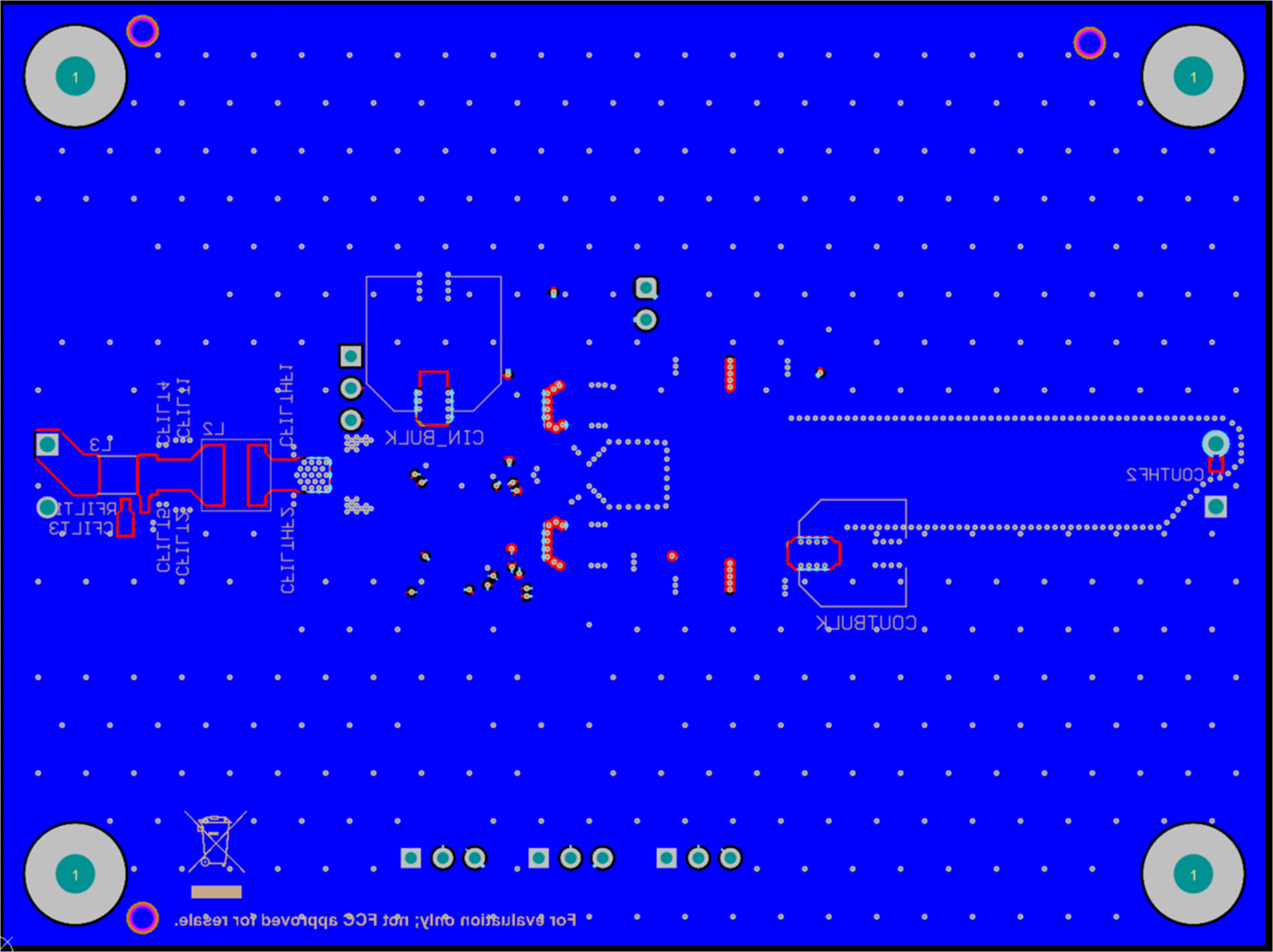 Figure 5-6 Bottom layer and bottom silkscreen