SNVU738 March   2022 LM5157 , LM5157-Q1 , LM51571-Q1


  1.   Trademarks
  2. 1Features and Electrical Performance
    1. 1.1 Electrical Parameters
    2. 1.2 EVM Power Derating Curve
    3. 1.3 Terminals and Signal Test Points
  3. 2Application Schematic
  4. 3EVM Picture
  5. 4Test Setup and Procedure
    1. 4.1 Bench Setup
    2. 4.2 Test Equipment
    3. 4.3 Precautions
  6. 5Test Data
    1. 5.1 Efficiency
    2. 5.2 Output Regulation
    3. 5.3 Thermal Performance
    4. 5.4 Typical Power Up
    5. 5.5 Output Ripple Voltage
    6. 5.6 Step Load Response
    7. 5.7 Bode Plots
  7. 6Schematics
  8. 7Bill of Materials
  9. 8Board Layout

Board Layout

The EVM PC Board consists of two copper layers, and the board includes various headers for flexible configurations suitable for different applications. Figure 8-1 through Figure 8-4 show the EVM PCB artwork.
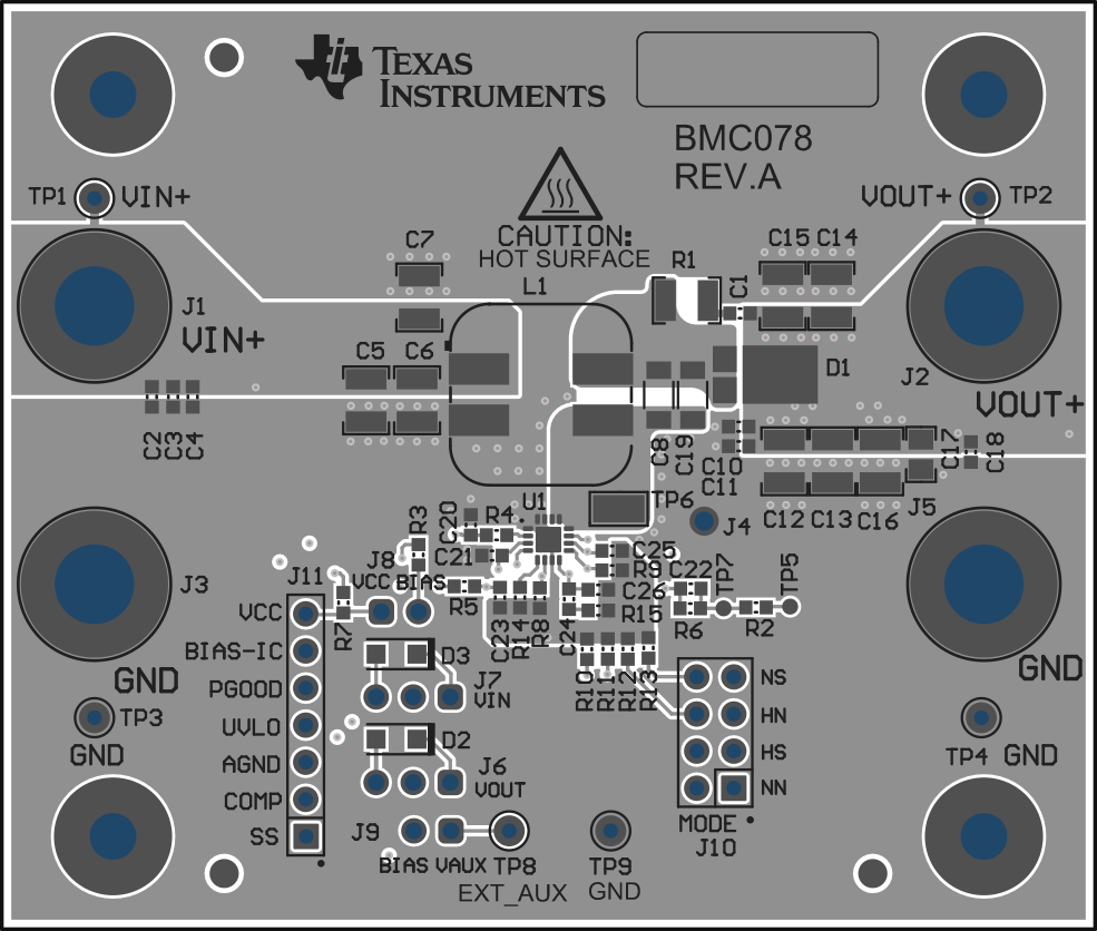
GUID-20220215-SS0I-HFC4-3SCV-386CKC7QJRT9-low.pngFigure 8-1 EVM Top Layer Silkscreen (view from top)
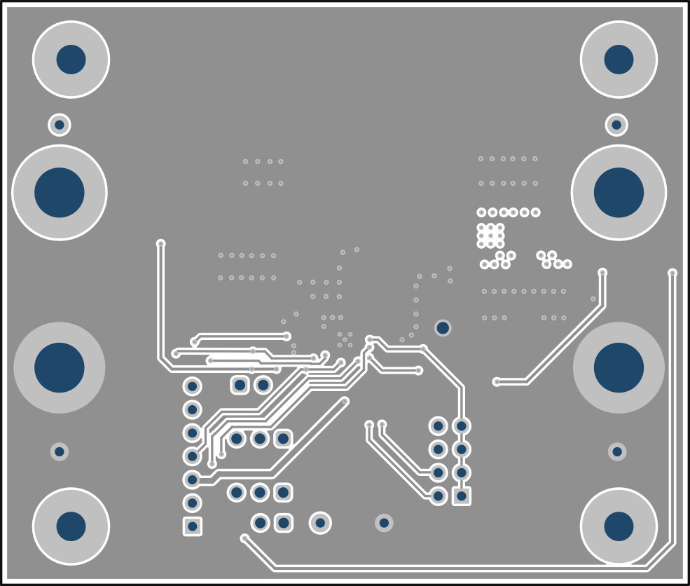
GUID-20220215-SS0I-CCLZ-TNMX-HCMPD033D4HH-low.pngFigure 8-3 EVM Middle Layer 2 (view from top)
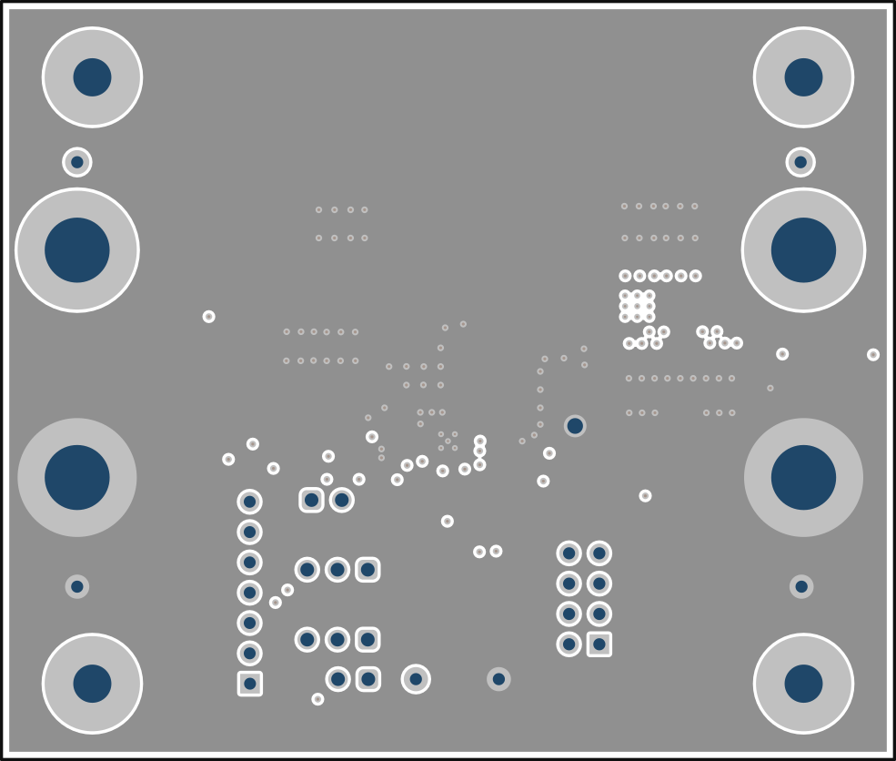
GUID-20220215-SS0I-WVTR-9SJT-7N46RTZSFGZ4-low.pngFigure 8-2 EVM Middle Layer 1 (view from top)
Figure 8-4 EVM Bottom Layer Silkscreen (view from bottom)