SPRADE1 March 2024 AM2434
3 Verification
To verify the accuracy and bandwidth of serial port data transmission, GPIO direct mode was applied for TX/RX loopback test. R5F stores 64 bytes of data to TCM at address 0x78000000. PRU0 queries TCM in periodic tasks and transmits data, clears the frame header data after transmission to avoid repeated. Meanwhile, PRU1 re-stores the received data to TCM at address 0x78000040 to verify the accuracy of the data received by comparing the transmitted and received data. oscilloscope measures the transmission bandwidth on the transmit side. The test results are shown in Figure 3-1 and Figure 3-2.
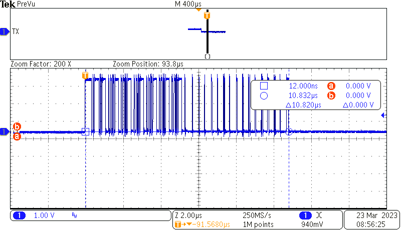 Figure 3-1 64 Bytes Transmit Time
As shown in Figure 3-1, bandwidth= length of data/time=512 bit/10.82μs=47.32Mbps.
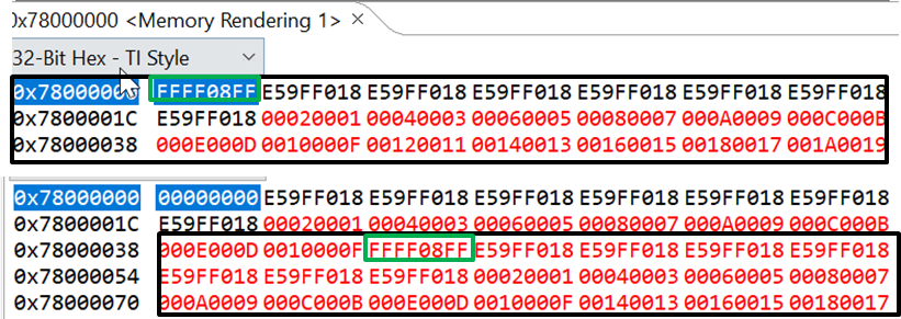 Figure 3-2 Transmit and Receive Data
Comparison
Figure 3-2 Transmit and Receive Data
ComparisonPRU_GPIO shift mode is similar to direct mode, 64bytes of TX/RX loopback test was performed, PRU0 in shift out mode, PRU1 in shift in mode, and transmit data is stored at 0x78000114 on R5F TCM. After data reception is complete, stored at 0x78000180.
Figure 3-4 shows that the PRU1 core received the correct data without errors.
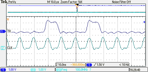 Figure 3-3 Shift Mode
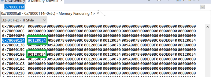 Figure 3-4 Transmit/Receive Data
Comparison
Figure 3-4 Transmit/Receive Data
ComparisonThe goal was to use GPIO shift out mode to achieve a 100Mbit data rate with serial communication.Figure 3-3 shows that CLK_OUT clock period is 10MHz and there is no error bit between transmit and receive data, which proves the validity of the serial communication. And to improve the reliability of serial communication, the CRC hardware accelerator is integrated inside the PRU_ICSSG to add CRC checksum after each communication frame.
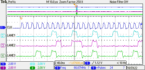 Figure 3-5 4-Lane Parallel Data
Transmission
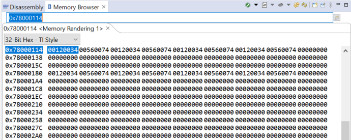 Figure 3-6 Transmit/Receive Data
Comparison
Figure 3-6 Transmit/Receive Data
ComparisonTo shows the parallel port performance, TX/RX loopback experiment was performed, transmit data is stored at 0x78000114 on R5F TCM. After data reception is complete, stored at 0x78000180. In this case, the clock cycle is equal to 5 PRU cycle, and bandwidth = length of data/time = 4 bits/cycle / (3ns/clock×5clocks/cycle)= 266.4Mbps. As more PRU GPI/GPO signals are used, the data throughput goes up. For example, a bandwidth of 1Gbps could be achieved with 1 clock signal and 15 data lines: bandwidth = length of data/time = 15 bits/cycle / (3ns/clock×5clocks/cycle) = 1Gbps.