SPRADG4A January   2024  – April 2024


  1.   1
  2.   Abstract
  3.   Trademarks
  4. 1General Texas Instruments High Voltage Evaluation (TI HV EVM) User Safety Guidelines
  5. 2Introduction
  6. 3System Description
    1. 3.1 Key System Specifications
  7. 4System Overview
    1. 4.1 Block Diagram
    2. 4.2 Basic Operation
    3. 4.3 System Design Theory
      1. 4.3.1 Peak Current Mode Control (PCMC) Implementation
      2. 4.3.2 Zero Voltage Switching (ZVS) or Low Voltage Switching (LVS)
      3. 4.3.3 Synchronous Rectification
      4. 4.3.4 Slope Compensation
  8. 5Hardware
    1. 5.1 Hardware Overview
    2. 5.2 Hardware and Test Instruments Required
    3. 5.3 TMDSCNCD263 controlCARD™ Changes
  9. 6Software
    1. 6.1 Getting Started With Firmware
      1. 6.1.1 Opening the Code Composer Studio Project
      2. 6.1.2 Software Architecture
      3. 6.1.3 Project Folder Structure
    2. 6.2 SysConfig Setup
      1. 6.2.1 EPWM Configuration
      2. 6.2.2 ADC Configuration
      3. 6.2.3 CMPSS Configuration
    3. 6.3 Incremental Builds
      1. 6.3.1 Procedure for Running the Incremental Builds - PCMC
        1. 6.3.1.1 Lab 1: Phase Overlapping Check With Open Current and Voltage Loop
          1. 6.3.1.1.1 Objective of Lab 1
          2. 6.3.1.1.2 Overview of Lab 1
          3. 6.3.1.1.3 Procedure of Lab 1
            1. 6.3.1.1.3.1 Start CCS and Open a Project for Lab 1
            2. 6.3.1.1.3.2 Build and Load the Project for Lab 1
            3. 6.3.1.1.3.3 Debug Environment Windows for Lab 1
            4. 6.3.1.1.3.4 Run the Code for Lab 1
        2. 6.3.1.2 Lab 2: Closed Current and Open Voltage Loop
          1. 6.3.1.2.1 Objective of Lab 2
          2. 6.3.1.2.2 Overview of Lab 2
          3. 6.3.1.2.3 Procedure of Lab 2
            1. 6.3.1.2.3.1 Build and Load Project for Lab 2
            2. 6.3.1.2.3.2 Debug Environment Windows for Lab 2
            3. 6.3.1.2.3.3 Run the Code for Lab 2
        3. 6.3.1.3 Lab 3: Closed Current and Closed Voltage Loop
          1. 6.3.1.3.1 Objective of Lab 3
          2. 6.3.1.3.2 Overview of Lab 3
          3. 6.3.1.3.3 Procedure of Lab 3
            1. 6.3.1.3.3.1 Build and Load Project for Lab 3
            2. 6.3.1.3.3.2 Debug Environment Windows for Lab 3
            3. 6.3.1.3.3.3 Run the Code for Lab 3
  10. 7Testing and Results
    1. 7.1 Lab 0: Basic PWM Check
    2. 7.2 Lab 1: Phase Overlapping Check With Open Current and Voltage Loop
    3. 7.3 Lab 2: Closed Current and Open Voltage Loop
    4. 7.4 Lab 3: Closed Current and Closed Voltage Loop
  11. 8References
  12. 9Revision History

Lab 0: Basic PWM Check

Lab 0 can be run on the AM263x controlCARD and docking station. To execute Lab 0, build the code by following the steps mentioned in Section 6.3.1.1.3.2.

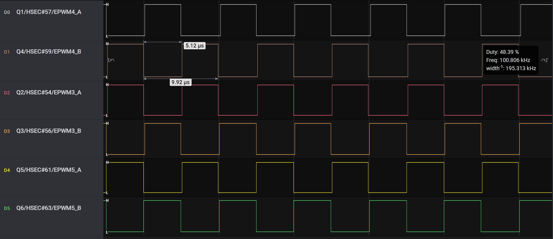
Connect the ADC4_AIN0, ADC1_AIN1, ADC3_AIN1, ADC3_AIN2 pins of the controlCARD docking station to ground point. Connect the EPWM3, EPWM4, EPWM5 pins of the controlCARD docking station to a logic analyzer to view the PWM waveforms.

  • ADC4_AIN0 – Pins 25
  • ADC1_AIN1 – Pins 18
  • ADC3_AIN1 – Pins 30
  • ADC3_AIN2 – Pins 32
  • EPWM3 – Pins 54, 56
  • EPWM4 – Pins 57, 59
  • EPWM5 – Pins 61, 63

Figure 7-1 shows the expected PWM waveforms.
GUID-B18F0341-84E9-44D2-82B9-9E8DE208A836-low.png Figure 7-1 PWM Waveforms