SPRS698J November 2010 – September 2021 TMS320F28062 , TMS320F28062-Q1 , TMS320F28062F , TMS320F28062F-Q1 , TMS320F28063 , TMS320F28064 , TMS320F28065 , TMS320F28066 , TMS320F28066-Q1 , TMS320F28067 , TMS320F28067-Q1 , TMS320F28068F , TMS320F28068M , TMS320F28069 , TMS320F28069-Q1 , TMS320F28069F , TMS320F28069F-Q1 , TMS320F28069M , TMS320F28069M-Q1
PRODUCTION DATA
- 1 Features
- 2 Applications
- 3 Description
- 4 Revision History
- 5 Device Comparison
- 6 Terminal Configuration and Functions
-
7 Specifications
- 7.1 Absolute Maximum Ratings
- 7.2 ESD Ratings – Commercial
- 7.3 ESD Ratings – Automotive
- 7.4 Recommended Operating Conditions
- 7.5 Power Consumption Summary
- 7.6 Electrical Characteristics
- 7.7 Thermal Resistance Characteristics
- 7.8 Thermal Design Considerations
- 7.9 Debug Probe Connection Without Signal Buffering for the MCU
- 7.10 Parameter Information
- 7.11 Test Load Circuit
- 7.12 Power Sequencing
- 7.13 Clock Specifications
- 7.14 Flash Timing
-
8 Detailed Description
- 8.1
Overview
- 8.1.1 CPU
- 8.1.2 Control Law Accelerator (CLA)
- 8.1.3 Viterbi, Complex Math, CRC Unit (VCU)
- 8.1.4 Memory Bus (Harvard Bus Architecture)
- 8.1.5 Peripheral Bus
- 8.1.6 Real-Time JTAG and Analysis
- 8.1.7 Flash
- 8.1.8 M0, M1 SARAMs
- 8.1.9 L4 SARAM, and L0, L1, L2, L3, L5, L6, L7, and L8 DPSARAMs
- 8.1.10 Boot ROM
- 8.1.11 Security
- 8.1.12 Peripheral Interrupt Expansion (PIE) Block
- 8.1.13 External Interrupts (XINT1 to XINT3)
- 8.1.14 Internal Zero Pin Oscillators, Oscillator, and PLL
- 8.1.15 Watchdog
- 8.1.16 Peripheral Clocking
- 8.1.17 Low-power Modes
- 8.1.18 Peripheral Frames 0, 1, 2, 3 (PFn)
- 8.1.19 General-Purpose Input/Output (GPIO) Multiplexer
- 8.1.20 32-Bit CPU-Timers (0, 1, 2)
- 8.1.21 Control Peripherals
- 8.1.22 Serial Port Peripherals
- 8.2 Memory Maps
- 8.3 Register Maps
- 8.4 Device Debug Registers
- 8.5 VREG, BOR, POR
- 8.6 System Control
- 8.7 Low-power Modes Block
- 8.8 Interrupts
- 8.9
Peripherals
- 8.9.1 CLA Overview
- 8.9.2 Analog Block
- 8.9.3 Detailed Descriptions
- 8.9.4 Serial Peripheral Interface (SPI) Module
- 8.9.5 Serial Communications Interface (SCI) Module
- 8.9.6
Multichannel Buffered Serial Port (McBSP) Module
- 8.9.6.1
McBSP Electrical Data/Timing
- 8.9.6.1.1 McBSP Transmit and Receive Timing
- 8.9.6.1.2
McBSP as SPI Master or Slave Timing
- 8.9.6.1.2.1 McBSP as SPI Master or Slave Timing Requirements (CLKSTP = 10b, CLKXP = 0)
- 8.9.6.1.2.2 McBSP as SPI Master or Slave Switching Characteristics (CLKSTP = 10b, CLKXP = 0)
- 8.9.6.1.2.3 McBSP as SPI Master or Slave Timing Requirements (CLKSTP = 11b, CLKXP = 0)
- 8.9.6.1.2.4 McBSP as SPI Master or Slave Switching Characteristics (CLKSTP = 11b, CLKXP = 0)
- 8.9.6.1.2.5 McBSP as SPI Master or Slave Timing Requirements (CLKSTP = 10b, CLKXP = 1)
- 8.9.6.1.2.6 McBSP as SPI Master or Slave Switching Characteristics (CLKSTP = 10b, CLKXP = 1)
- 8.9.6.1.2.7 McBSP as SPI Master or Slave Timing Requirements (CLKSTP = 11b, CLKXP = 1)
- 8.9.6.1.2.8 McBSP as SPI Master or Slave Switching Characteristics (CLKSTP = 11b, CLKXP = 1)
- 8.9.6.1
McBSP Electrical Data/Timing
- 8.9.7 Enhanced Controller Area Network (eCAN) Module
- 8.9.8 Inter-Integrated Circuit (I2C)
- 8.9.9 Enhanced Pulse Width Modulator (ePWM) Modules (ePWM1 to ePWM8)
- 8.9.10 High-Resolution PWM (HRPWM)
- 8.9.11 Enhanced Capture Module (eCAP1)
- 8.9.12 High-Resolution Capture Modules (HRCAP1 to HRCAP4)
- 8.9.13 Enhanced Quadrature Encoder Modules (eQEP1, eQEP2)
- 8.9.14 JTAG Port
- 8.9.15 General-Purpose Input/Output (GPIO) MUX
- 8.9.16 Universal Serial Bus (USB)
- 8.1
Overview
- 9 Applications, Implementation, and Layout
- 10Device and Documentation Support
- 11Mechanical, Packaging, and Orderable Information
8.9.2.1.1 Features
The core of the ADC contains a single 12-bit converter fed by two sample-and-hold circuits. The sample-and-hold circuits can be sampled simultaneously or sequentially. These, in turn, are fed by a total of up to 16 analog input channels. The converter can be configured to run with an internal band-gap reference to create true-voltage based conversions or with a pair of external voltage references (VREFHI/VREFLO) to create ratiometric-based conversions.
Contrary to previous ADC types, this ADC is not sequencer-based. The user can easily create a series of conversions from a single trigger. However, the basic principle of operation is centered around the configurations of individual conversions, called SOCs, or Start-Of-Conversions.
Functions of the ADC module include:
- 12-bit ADC core with built-in dual sample-and-hold (S/H)
- Simultaneous sampling or sequential sampling modes
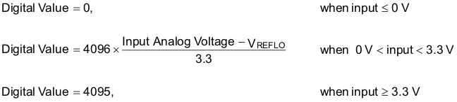
- Full range analog input: 0 V to
3.3 V fixed, or VREFHI/VREFLO ratiometric. The digital
value of the input analog voltage is derived by:
- Internal Reference
(VREFLO = VSSA. VREFHI must not
exceed VDDA when using either internal or external reference
modes.)
- External Reference
(VREFHI/VREFLO connected to external
references. VREFHI must not exceed VDDA when using
either internal or external reference modes.)
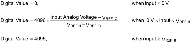
- Internal Reference
(VREFLO = VSSA. VREFHI must not
exceed VDDA when using either internal or external reference
modes.)
- Up to 16-channel, multiplexed inputs
- 16 SOCs, configurable for trigger, sample window, and channel
- 16 result registers (individually addressable) to store conversion values
- Multiple trigger sources
- S/W – software immediate start
- ePWM 1–8
- GPIO XINT2
- CPU Timer 0, CPU Timer 1, CPU Timer 2
- ADCINT1, ADCINT2
- 9 flexible PIE interrupts, can configure interrupt request after any conversion
| REGISTER NAME | ADDRESS | SIZE (×16) |
EALLOW PROTECTED |
DESCRIPTION |
|---|---|---|---|---|
| ADCCTL1 | 0x7100 | 1 | Yes | Control 1 Register |
| ADCCTL2 | 0x7101 | 1 | Yes | Control 2 Register |
| ADCINTFLG | 0x7104 | 1 | No | Interrupt Flag Register |
| ADCINTFLGCLR | 0x7105 | 1 | No | Interrupt Flag Clear Register |
| ADCINTOVF | 0x7106 | 1 | No | Interrupt Overflow Register |
| ADCINTOVFCLR | 0x7107 | 1 | No | Interrupt Overflow Clear Register |
| INTSEL1N2 | 0x7108 | 1 | Yes | Interrupt 1 and 2 Selection Register |
| INTSEL3N4 | 0x7109 | 1 | Yes | Interrupt 3 and 4 Selection Register |
| INTSEL5N6 | 0x710A | 1 | Yes | Interrupt 5 and 6 Selection Register |
| INTSEL7N8 | 0x710B | 1 | Yes | Interrupt 7 and 8 Selection Register |
| INTSEL9N10 | 0x710C | 1 | Yes | Interrupt 9 Selection Register (reserved Interrupt 10 Selection) |
| SOCPRICTL | 0x7110 | 1 | Yes | SOC Priority Control Register |
| ADCSAMPLEMODE | 0x7112 | 1 | Yes | Sampling Mode Register |
| ADCINTSOCSEL1 | 0x7114 | 1 | Yes | Interrupt SOC Selection 1 Register (for 8 channels) |
| ADCINTSOCSEL2 | 0x7115 | 1 | Yes | Interrupt SOC Selection 2 Register (for 8 channels) |
| ADCSOCFLG1 | 0x7118 | 1 | No | SOC Flag 1 Register (for 16 channels) |
| ADCSOCFRC1 | 0x711A | 1 | No | SOC Force 1 Register (for 16 channels) |
| ADCSOCOVF1 | 0x711C | 1 | No | SOC Overflow 1 Register (for 16 channels) |
| ADCSOCOVFCLR1 | 0x711E | 1 | No | SOC Overflow Clear 1 Register (for 16 channels) |
| ADCSOC0CTL to ADCSOC15CTL | 0x7120 – 0x712F | 1 | Yes | SOC0 Control Register to SOC15 Control Register |
| ADCREFTRIM | 0x7140 | 1 | Yes | Reference Trim Register |
| ADCOFFTRIM | 0x7141 | 1 | Yes | Offset Trim Register |
| COMPHYSTCTL | 0x714C | 1 | Yes | Comparator Hysteresis Control Register |
| ADCREV | 0x714F | 1 | No | Revision Register |
| REGISTER NAME | ADDRESS | SIZE (×16) |
EALLOW PROTECTED |
DESCRIPTION |
|---|---|---|---|---|
| ADCRESULT0 to ADCRESULT15 | 0xB00 to 0xB0F | 1 | No | ADC Result 0 Register to ADC Result 15 Register |
 Figure 8-21 ADC
Connections
Figure 8-21 ADC
ConnectionsADC Connections if the ADC is Not Used
TI recommends keeping the connections for the analog power pins, even if the ADC is not used. Following is a summary of how the ADC pins should be connected, if the ADC is not used in an application:
- VDDA – Connect to VDDIO
- VSSA – Connect to VSS
- VREFLO – Connect to VSS
- ADCINAn, ADCINBn, VREFHI – Connect to VSSA
When the ADC module is used in an application, unused ADC input pins should be connected to analog ground (VSSA).
TI recommends that unused ADCIN pins which are multiplexed with AIO function be grounded through a 1-kΩ resistor. This recommendation is intended to prevent any inadvertent software activation of the AIO output logic-high driving directly to ground; this condition can cause permanent device damage by exceeding IOH Absolute Maximum.
When the ADC is not used, be sure that the clock to the ADC module is not turned on to realize power savings.