SPRUJ66A February 2023 – December 2023
- 1
- Abstract
- Trademarks
- 1EVM Revisions and Assembly Variants
- 2Inside the Box
- 3EMC, EMI, and ESD Compliance
-
4System Description
- 4.1 Key Features
- 4.2 Functional Block Diagram
- 4.3 AM62A Low Power SK EVM Interface Mapping
- 4.4 Power ON/OFF Procedures
- 4.5
Peripheral and Major Component Description
- 4.5.1 Clocking
- 4.5.2 Reset
- 4.5.3 CSI Interface
- 4.5.4 Audio Codec Interface
- 4.5.5 HDMI Display Interface
- 4.5.6 JTAG Interface
- 4.5.7 Test Automation Header
- 4.5.8 UART Interface
- 4.5.9 USB Interface
- 4.5.10 Memory Interfaces
- 4.5.11 Ethernet Interface
- 4.5.12 GPIO Port Expander
- 4.5.13 GPIO Mapping
- 4.5.14 Power
- 4.5.15 AM62A Low Power SK EVM User Setup and Configuration
- 4.5.16 Expansion Headers
- 4.5.17 I2C Address Mapping
- 5Revision History
4.5.1 Clocking
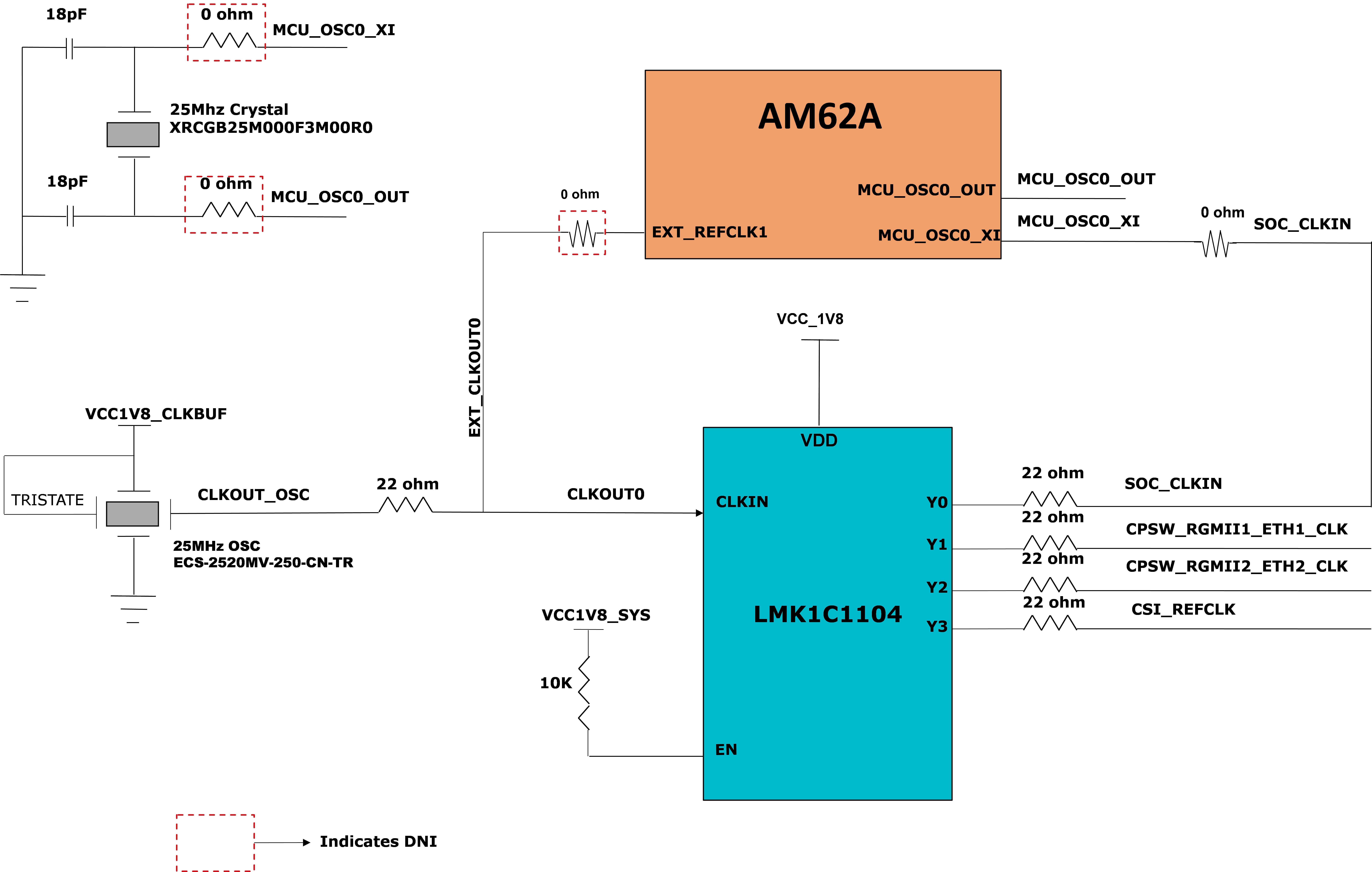
The Clock architecture of AM62A-Low Power SK EVM is shown below.
 Figure 4-9 Clock architecture
A clock generator of part number LMK1C1104PWR is used to drive the 25MHz clock to the SOC, two Ethernet PHYs & CSI Camera devices. LMK1C1104PWR is a 1:4 LVCMOS clock buffer, which takes the 25MHz crystal/LVCMOS referenceinput and provides four 25MHz LVCMOS clock outputs. The source for the clock buffer shall be either the CLKOUT0 pin from the SOC or a 25MHz oscillator, the selection of which is made using a set of resistors. By default, an oscillator is used as an input to the clock buffer on the AM62A-Low Power SK EVM. Output Y1 and Y2 of the clock buffer are used as reference clock inputs for the two Gigabit Ethernet PHYs. Output Y3 of the clock buffer is used as a reference clock input for CSI Camera interface.
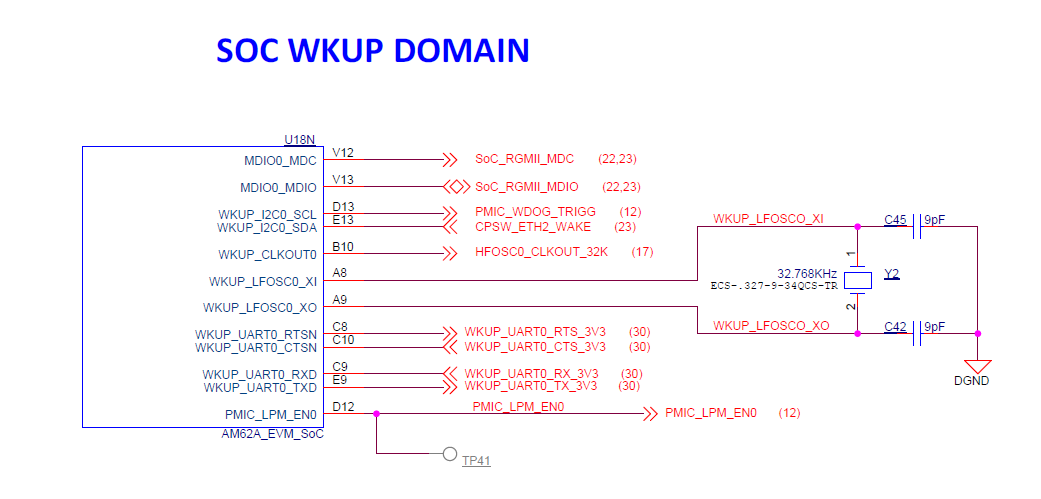
There is one external crystal (32.768 KHz) attached to the AM62A SOC to provide clock to its WKUP domain.
 Figure 4-10 SoC WKUP Domain Clock