SPRZ267J March 2009 – September 2020 TMS320C28341 , TMS320C28342 , TMS320C28343 , TMS320C28343-Q1 , TMS320C28344 , TMS320C28345 , TMS320C28346 , TMS320C28346-Q1
3 Device Markings
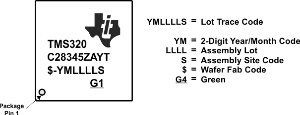
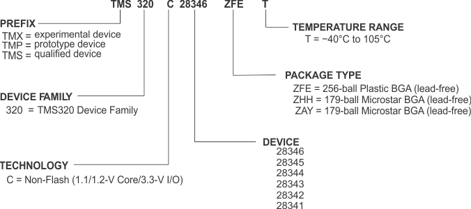
Figure 3-1 provides examples of the 2834x device markings and defines each of the markings. The device revision can be determined by the symbols marked on the top of the package as shown in Figure 3-1. Some prototype devices may have markings different from those illustrated. Figure 3-2 shows the device nomenclature.
 Figure 3-1 Examples
of Device Markings
Figure 3-1 Examples
of Device MarkingsTable 3-1 Determining Silicon Revision From Lot Trace Code
| LETTER FOLLOWING WAFER FAB CODE |
SILICON REVISION | REVISION ID Address: 0x0883 |
COMMENTS |
|---|---|---|---|
| Blank (no letter follows the Wafer Fab Code) |
Indicates Revision 0 | 0x0000 | This silicon revision is available as TMS. |
 Figure 3-2 Device
Nomenclature