SSZT122 October 2021 LM2903 , TLV3605 , TLV7012
Comparators are fundamental analog components found in nearly every application. One way to describe comparators is that they are 1-bit ADCs: They have two inputs, with one typically used as a voltage reference and the other an input voltage signal. Depending on which input is the reference and what the input voltages are, the comparator output will toggle high or low. These components have many uses, especially in mixed-signal and control applications such as over- and under-voltage detection and temperature sensing.
While the concept of comparators is simple, there are several common design challenges that occur during implementation. To address these challenges, this article is the first installment in a three-part series covering the three most common design considerations designers must address for optimal comparator performance – beginning with chatter.
What is chatter?
To demonstrate the phenomena of chatter, I set up the LM2903 dual differential comparator in a noninverting configuration (Figure 1), with noise added to a 1-V peak-to-peak triangle wave centered about the reference voltage (VREF). There are multiple, rapid transitions when the input voltage (VIN) is around the reference voltage present on IN–, as shown in Figure 2.
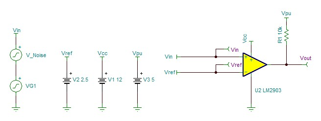 Figure 1 Noninverting Comparator
Setup
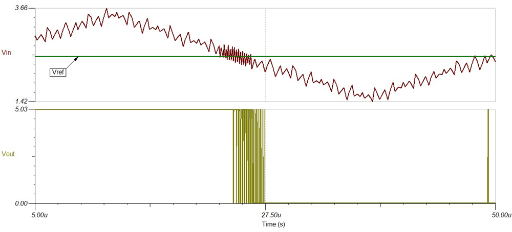 Figure 2 Comparator Chatter
These rapid transitions are sometimes mistaken for oscillation; however, this behavior is actually called chatter. Chatter does not represent a defect in the device; it is normal. From the perspective of the comparator, it is seeing a signal go above and below the threshold of the reference. Even very slight variations around the reference will cause the output to transition states. Comparators have relatively fast response times and will change states as long as the signal variations are within its maximum toggle frequency.
Chatter causes and effects
The primary cause of chatter is noise present in the system, which can come from several sources, including the input, VREF, the power supply, components, the prototyping board – even the comparator itself. It is even possible for chatter to occur solely from the noise of the comparator, with the inputs tied together for approximately 0 mV of internal offset voltage (VOS). Regardless of the noise source, the comparator will experience chatter on the output, since the input voltage will go above and below the reference in rapid random succession.
Chatter on the output is a serious problem if it goes unchecked. Unwanted output-state transitions can lead to misinformation and control for downstream devices such as FET switches, causing erratic system behavior and potentially rendering a system ineffective. For example, chatter can cause a comparator controlling the enable pin of a DC/DC converter to repeatedly power up and shut the system down. Additionally, slow-moving signals such as battery voltages or temperature sensor voltages have greater susceptibility to chatter, since the signal crosses the reference slowly and can incur more reference crossing from the noise. This can unintentionally activate and deactivate under- or overvoltage and temperature-protection circuitry.
Chatter solutions
There are two primary ways to combat chatter, each with secondary subset options. The first option is to implement external hysteresis through positive feedback. External hysteresis effectively increases the offset voltage thresholds above and below the reference. Figure 3 shows a comparator in a noninverting configuration with external hysteresis, and its transfer characteristic curve.
 Figure 3 Noninverting Comparator with
External Hysteresis
Figure 3 Noninverting Comparator with
External HysteresisAnother way to eliminate chatter is to use a comparator that has integrated or variable hysteresis such as the TLV7012. See Figure 4 for the data-sheet specification. Integrated hysteresis can also have the added benefit of saving space on a printed circuit board with tight space constraints by eliminating components from the layout.
 Figure 4 TLV7012 Hysteresis
Specification
Figure 4 TLV7012 Hysteresis
SpecificationThe TLV3603 and TLV3605, for example, have a pin to provide adjustable internal hysteresis. The functionality of the LE/HYS pin (see Figure 5) enables variable hysteresis depending on the resistor value connected between the pin and the emitter supply voltage (VEE), where decreasing the resistance increases hysteresis up to a point. If the hysteresis provided by the chip is not sufficient (larger than the noise present in the system), it is still possible to implement external hysteresis.
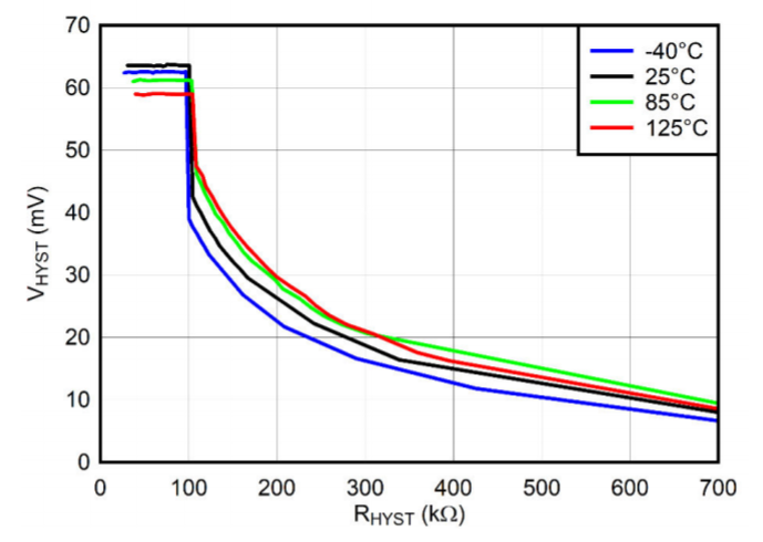 Figure 5 VHYST (Millivolts)
vs. RHYST (Kilo-ohms)
Figure 5 VHYST (Millivolts)
vs. RHYST (Kilo-ohms)For higher-speed systems where DC accuracy is paramount, using a feedback capacitor instead of a resistor to provide short-term hysteresis will implement AC hysteresis without affecting the threshold voltages. We will expand upon the concept of AC hysteresis in a future article.
The second option to reduce the likelihood of chatter is to filter the input signal, the reference, or both. Properly bypassing the supply will also help minimize glitches from large current spikes. The downside to filtering the inputs is that it delays the signal and can violate strict system timing requirements. It is possible, however, that filtering the inputs can eliminate chatter without changing the voltage thresholds for state transition.
Figure 6 shows a possible filtering scheme in conjunction with hysteresis to eliminate chatter below. Note how C1 is crossed out, since applying capacitance to the noninverting node when implementing positive feedback can cause a delay in the feedback and potentially negate it entirely. I recommend placing any bypass or filtering capacitors as close to the pin as the layout permits for maximum effectiveness. Using multiple bypass capacitors in different decade ranges (for example, 1 µF, 100 nF and 100 pf) will provide the best noise reduction across frequency ranges.
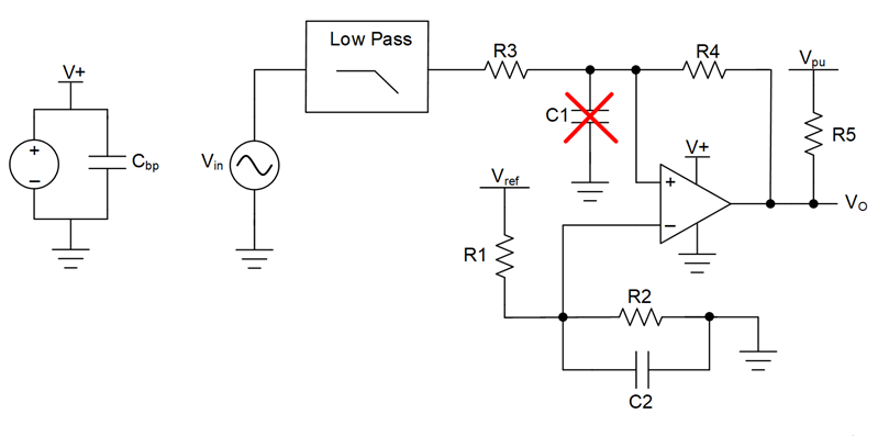 Figure 6 Noninverting Comparator with
External Hysteresis and Filtering
Figure 6 Noninverting Comparator with
External Hysteresis and FilteringFigure 7 and Figure 8 show the resultant waveform after applying hysteresis, filtering and proper bypassing, as well as the circuit configuration. Using equations from "Non-Inverting Comparator with Hysteresis Circuit," with a chosen value of R1 = 100 kΩ, R5 = 10 kΩ, VHYST = 500 mV, VO(max) = 5 V, VO(min) = 110 mV and VREF = 2.5, calculated values of R2 = 100 kΩ, R3 = 49.9 kΩ and R4 = 442 kΩ. Note that all resistor values are rounded to the nearest 1% standard resistor value.
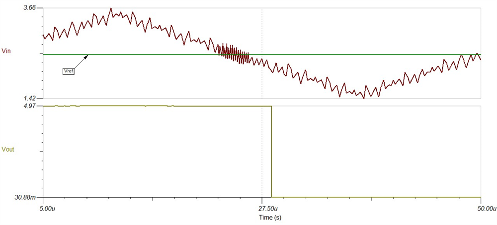 Figure 7 Comparator Chatter Resolved
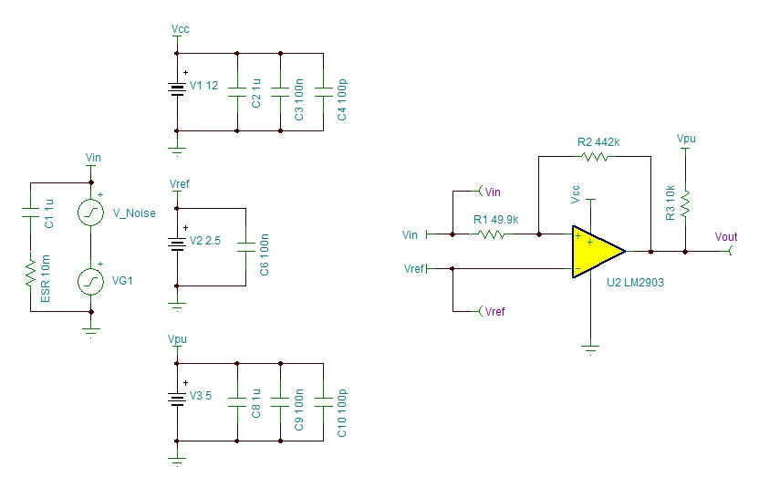 Figure 8 Noninverting Comparator with External Hysteresis and Filtering Setup
Conclusion
In order to increase resistance to noise (and consequently chatter), some timing and precision specifications may be unattainable. Implementing either filtering or hysteresis improves system performance, but I recommend implementing both for the greatest chatter reduction. Keep in mind that implementing hysteresis will change the threshold voltages, so choose them to reflect the requirements of the system. Also note how filtering effects the system's timing constraints.
Creating resistance to noise is an important aspect of every system and will minimize comparator glitches and unwanted performance. In the second installment of this series, we will discuss input common-mode voltage range.