SSZT206 December 2020 CSD17576Q5B , CSD19532Q5B
Power metal-oxide semiconductor field-effect transistor (MOSFET) data sheets provide useful information such as key specifications, ratings and characteristics to help you confirm that the device will operate as intended. You may have questions about how a parameter varies, however, so in this article I’ll explain not just what’s in the data sheet but more importantly, what’s not.
MOSFET data-sheet review
 Figure 1 First page of the CSD17576Q5B NexFET™ data sheet
The second page of the data sheet includes the table of contents and the revision history. Next are the specifications tables, electrical characteristics and thermal information, followed by graphs displaying the typical MOSFET characteristics. Then there is a section on device and documentation support. The data sheet includes the mechanical, packaging and orderable information in its final section. Unless otherwise noted, all specifications and ratings are at an ambient temperature, TA = 25°C.
Temperature dependence
Static characteristics
 Figure 2 The electrical characteristics
table in the CSD17576Q5B NexFET™ data sheet
Figure 2 The electrical characteristics
table in the CSD17576Q5B NexFET™ data sheetFigure 3 is the temperature variation of BVDSS for two power MOSFETs: the CSD17576Q5B 30-V trench FET and the CSD19532Q5B 100-V superjunction device; the curves in Figure 3 show the temperature dependence for BVDSS as well as IDSS and IGS. As the temperature increases, the breakdown voltage for both increases nearly linearly. The slope of the line is the positive temperature coefficient of BVDSS and will differ based on the FET’s process technology and voltage rating. Notice that the positive temperature coefficient is less for the CSD19532Q5B than for the CSD17576Q5B.
; CSD19532Q5B (b)") Figure 3 Normalized BVDSS
vs. temperature: CSD17576Q5B (a); CSD19532Q5B (b)
Figure 3 Normalized BVDSS
vs. temperature: CSD17576Q5B (a); CSD19532Q5B (b)Figure 4 shows the temperature dependence of IDSS for the CSD17576Q5B and CSD19532Q5B. The lower-voltage FET, the CSD17576Q5B, displays more variation over the temperature range from -55°C to 150°C. For both devices, the plots tend to flatten out at low temperatures. This is not actual behavior but a test measurement system limitation at the very small currents being measures. The device physics dictate a continual downward trend at low temperatures.
; CSD19532Q5B (b)") Figure 4 Normalized IDSS vs.
temperature: CSD17576Q5B (a); CSD19532Q5B (b)
Figure 4 Normalized IDSS vs.
temperature: CSD17576Q5B (a); CSD19532Q5B (b)As shown in Figure 5 for the CD17576Q5B and CSD19532Q5B, IGSS also has a positive temperature variation. The relative increase in IGSS is greater for the CSD19532Q5B over the temperature range from -55°C to 150°C. Again, the flattening of the curves at low temperatures is caused by the resolution of the test measurement system.
; CSD19532Q5B (b)") Figure 5 Normalized IGSS vs.
temperature: CSD17576Q5B (a); CSD19532Q5B (b)
Figure 5 Normalized IGSS vs.
temperature: CSD17576Q5B (a); CSD19532Q5B (b)The last parameter, gfs, is also temperature-dependent. You can use the transfer curves from the CSD17576Q5B and CSD19532Q5B data sheets as shown in Figure 6 to estimate gfs using Equation 1:
gfs = ΔIDS/ΔVGS (1)
; CSD19532Q5B (b)") Figure 6 Transfer characteristics:
CSD17576Q5B (a); CSD19532Q5B (b)
Figure 6 Transfer characteristics:
CSD17576Q5B (a); CSD19532Q5B (b)Picking data points from the data-sheet curves, Table 1 lists the estimated values for gfs. You can see that transconductance has a negative temperature coefficient.
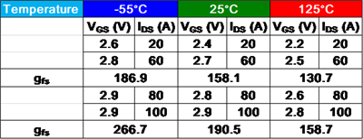
Table 1: Estimated gfs values for the CSD17576Q5B
You can make the same gfs estimates using the transfer characteristics for the CSD19532Q5B, as listed in Table 2.
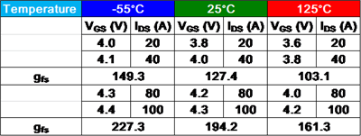
Table 2: Estimated gfs values for the CSD19532Q5B
Dynamic characteristics
 Figure 7 MOSFET model with parasitic elements
Diode characteristics
 Figure 8 Reverse-recovery current vs. temperature for two FETs
Safe operating area
; and CSD19532Q5B (b)") Figure 9 Maximum safe operating area at TA = 25°C: CSD17576Q5B (a); and CSD19532Q5B (b)
Figure 9 Maximum safe operating area at TA = 25°C: CSD17576Q5B (a); and CSD19532Q5B (b)The easiest approach is to use a linear derating factor. From the graph, determine the SOA current, IDS(SOA), at the voltage, VDS(SOA) and the pulse width of interest. Equation 2 calculates the SOA current at temperature T (°C) as:
IDS(SOA@T) = IDS(SOA) × (TJmax - T)/(TJmax - 25°C) (2)
Equation 2 yields 0 current when T = TJmax, specified in the data sheet.
Conclusion
Additional resources
- Check out these technical articles:
- “Understanding MOSFET data sheets, Part 1 – UIS/avalanche ratings.”
- “Understanding MOSFET data sheets, Part 5 – Switching
Parameters.”
- Visit the TI MOSFET support and training center.
- Read the white paper, “Novel Thermally Enhanced Power Package.”
- Review the application report, “3D packaging advancements drive performance, power and density in power devices.”
Reference
- Jahdi, Saeed, Olayiwola Alatise, Roozbeh Bonyadi, Petros Alexakis, Craig Fisher, Jose A. Ortiz Gonzalez, Li Ran, and Philip Mawby “An Analysis of the Switching Performance and Robustness of Power MOSFETs Body Diodes: A Technology Evaluation.” IEEE Transactions on Power Electronics 30, no. 5 (May 2015): pp. 2383-2394.