SSZT316 march 2020 TPS62840
Electromagnetic noise is any type of unwanted electromagnetic energy that contains sufficient intensity to distort a signal. When designing high-performance data-acquisition applications or any system with particularly sensitive signal paths, noise is therefore the opponent to beat.
On the power-supply side, high-efficiency DC/DC converters can be significant sources of noise due to their basic operational principles. They generate both low-frequency ripple at the converter’s switching frequency as well as high-frequency noise caused by the fast switching of voltages and currents in the converter power stage.
Examples of noise-reduction techniques used in combination with switching regulators include the implementation of additional filtering passive components, like snubber circuits, ferrite beads and feedthrough capacitors, or the inclusion of linear power sources like low-dropout regulators in the power path. While these schemes work well for most applications, they may have trade-offs in terms of efficiency, solution size and of course the cost of the total power solution, particularly in always-on applications like patient monitors, smart meters, smart sensors and Internet of Things systems.
Many applications will certainly benefit from a noise-free environment during data acquisition and/or radio-frequency (RF) communication events. However, power-supply designers need to consider if the efficiency (in other words, battery lifetime), board space and component cost trade-offs make sense for their design. In scenarios where this can prove problematic, modern DC/DC converters do offer features that help reduce the impact of design compromises. One example is the TPS62840 DC/DC converter, an ultra-low (60-nA) quiescent-current, high-efficiency, 750-mA step-down regulator designed to maximize battery lifetime in always-on applications.
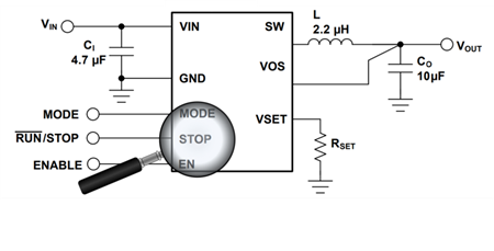
The TPS62840’s STOP input pin (see Figure 1) stops regulator switching both immediately (after the current switching cycle) and temporarily. During this time, the charge stored in the output capacitor powers the application; the regulator generates absolutely no ripple or switching noise. In those conditions, the application can perform distortion-free, precise data-acquisition and RF communication procedures.
 Figure 1 Typical application circuit
showing the STOP input pin
Figure 1 Typical application circuit
showing the STOP input pinOf course, it’s important to design the system in a way that the device turns back on before its output voltage reaches a system-critical level. As soon as a logic-low level is applied to the STOP pin, the regulator will immediately resume switching operation, without any startup and/or soft-start delay. Figure 2 illustrates the STOP feature for operating the DC/DC converter in pulse-frequency modulation (PFM) (Figure 2a) or forced pulse-width modulation (PWM) (Figure 2b).
 Figure 2 STOP mode operation for the
TPS62840 (where blue is the input signal for the STOP pin, magenta is the output
voltage and green is the inductor current) taken with VIN = 3.6 V,
VOUT = 1.8 V and IOUT = 10 mA in PFM operation (a);
and forced PWM operation (b). The measurements include COUT = 10
µF
Figure 2 STOP mode operation for the
TPS62840 (where blue is the input signal for the STOP pin, magenta is the output
voltage and green is the inductor current) taken with VIN = 3.6 V,
VOUT = 1.8 V and IOUT = 10 mA in PFM operation (a);
and forced PWM operation (b). The measurements include COUT = 10
µFHow long to undertake a noise-free measurement/RF communication event in STOP mode depends on the set output voltage VOUT,SET, the output capacitor value COUT, the required output current IOUT and the voltage tolerance of the application. In the examples of Figure 2 (VIN = 3.6 V, VOUT,SET = 1.8 V, IOUT = 10 mA, COUT = 10 µF), a voltage drop of about 50 mV is reached after a time t = 38 µs. In cases where a constant output current IOUT discharges the output capacitor COUT, you can estimate the output voltage behavior VOUT(t) in STOP mode as a function of time t with Equation 1:
When designing the power architecture of an always-on application with strong noise control requirements, make sure to check out the STOP function of the TPS62840. Combined with other features like 80% light-load efficiency at output currents as low as IOUT = 1 µA, or the possibility to select between 16 predefined output voltages with a single resistor connected to the VSET pin, the TPS62840 may help maximize your system’s battery lifetime while minimizing the amount of required additional components.
Additional resources
- Read these Analog Design Journal articles:
- Check out the Light Load Efficient, Low Noise Power Supply Reference Design for Wearables and IoT.
- Download the white paper, “Benefits of a Resistor-to-Digital Converter in Ultra-Low Power Supplies.”
- Learn more about “Deciphering low Iq: Using WEBENCH® to design near 100% duty cycle for ultra-low power applications.”