SSZT410 september 2019 TPS54228 , TPS562201 , TPS562231
Achieving a small power rail solution size is one of the highest priorities for embedded system engineers, especially for those designing industrial and communications equipment such as drones or routers. Compared to models released a few years ago, currently available drones are much lighter and have smaller fuselages, while routers are now more portable and compact with a built-in power adapter. As equipment size shrinks, engineers are looking for ways to shrink the power supply solution. In this technical article, I’ll provide a few tips to help you make your power rail design smaller, while demonstrating how to resolve the resulting thermal performance challenges.
Shrinking the package
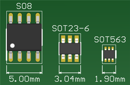
 Figure 1 Mechanical outline sizes of
three converter packages
Figure 1 Mechanical outline sizes of
three converter packagesApart from choosing a smaller package, another approach to reducing your solution size is to reduce the output inductor and capacitor. Equation 1 and Equation 2 calculate the output inductance (LOUT) and output capacitance (COUT), respectively.
where r is defined as the ratio of current ripple of inductor, V RIPPLE is the maximum allowed peak-to-peak ripple voltage and f sw is the switching frequency of the converter. Because L OUT and C OUT are both inversely proportional to f sw, the larger the switching frequency, the smaller the L OUT and C OUT. Smaller inductance or capacitance means engineers can select an inductor or a capacitor of a smaller size. Converters with a higher f sw can work with these smaller inductors and capacitors.
Addressing thermal performance
where P LOSS is the total power loss of the converter and R ΘJA is the junction-to-ambient thermal resistance. Consider a 2-A load converter with an average R DS(on) change from 100 mΩ to 50 mΩ. The power loss of this device will result in a 200-mW decrease, which will bring a 16°C cooldown on a typical SOT-563 board with a thermal resistance of 80°C/W. Therefore converters with a lower R DS(on) offer better working conditions at a lower temperature.
Turning theory to practice
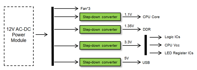
 Figure 2 Power-stage architecture of an
embedded system
Figure 2 Power-stage architecture of an
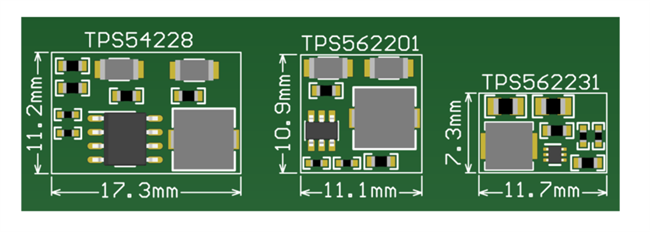
embedded systemThe TPS54228 has a 700-kHz frequency in an SO-8 package. The TPS562201 has a 580-kHz frequency in an SOT-23-6 package, and the TPS562231 has a 850-kHz frequency in an SOT-563 package. The TPS562231 has the highest frequency and the smallest IC package size. This solution size is about 142% smaller than the TPS562201, and 227% smaller than the TPS54228, as illustrated in Figure 3.
 Figure 3 Solution sizes of converters with different packages
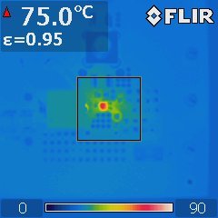
The R DS(on) of the integrated metal-oxide semiconductor field-effect transistor (MOSFET) in the TPS562231 is 95 mΩ (high side) and 55 mΩ (low side). Figure 4 is a thermal image of the full load temperature rise of a 12-V input on the TPS562231 evaluation board.
 Figure 4 Thermal image of the TPS562231 with a 12-V input voltage
In general, the TPS562231 works in an 850-kHz switching frequency sealed in a small SOT-563 package, which can help reduce the overall solution size. Its low on-resistance also allows for good thermal performance. It’s suitable for routers, drones, set-top boxes or any other embedded designs that require small solution sizes.
Additional resources
- Read the 3 tips for reducing wireless network interference in access point equipment technical article.
- Check out the Optimizing DC-DC Layout For SOT Package To Improve Thermal And Voltage Spike application note.
- Find out more about thermals in the SOT23 Package Thermal Consideration application note.