SSZT712 may 2018 LM53603 , LM53635-Q1 , LM61460-Q1 , LM65645-Q1 , LM70660 , LM706A0 , LM706A0-Q1 , LM70840 , LM70840-Q1 , LM70860 , LM70860-Q1 , LM70880 , LM70880-Q1 , LM73605 , LM76002 , LM76003 , LMR36006 , LMR36015
The origin of electromagnetic interference (EMI) in switched-mode power supplies can be traced back to the transient voltages (dv/dt) and currents (di/dt) generated during the switching of power metal-oxide semiconductor field-effect transistor (MOSFET) devices. With ever-growing demand for more power as well as higher switching frequencies, it is becoming increasingly challenging to address EMI in regards to device performance and meeting regulatory requirements. In this article, I’ll present an overview of the most widely used package types used for power electronics devices and their influence on EMI.
There are three common package types used in power electronics today:
- Thin-shrink small-outline package (TSSOP).
- Quad-flat no lead (QFN).
- Flip-chip on lead (FCOL QFN) or TI HotRod™ package.
TSSOP
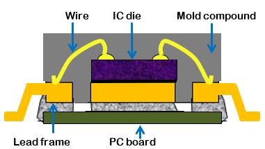 Figure 1 TSSOP Package Cross Section
The question is, how do all of these TSSOP characteristics affect device EMI performance? Increased parasitic inductance will result in larger overshoot on the switch node. Package parasitic components are just a part of the overall picture, however; board layout also plays a very important role.
Figure 2 is an oscilloscope screenshot showing a switch-node waveform on a DC/DC converter in TSSOP. Increased ringing on the switch node will have a direct effect on resulting EMI performance, making it more challenging to meet required EMI regulatory compliance (for example, Comité International Spécial des Perturbations Radioélectriques [CISPR] 25 class 5 requirements). The observed ringing frequency is in the 150MHz-250MHz range.
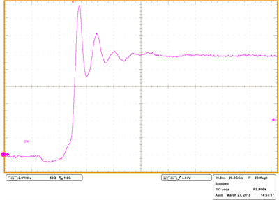 Figure 2 Switch Node Waveform for the TSSOP Package
QFN Package
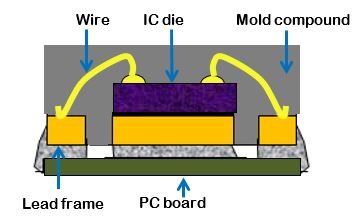 Figure 3 QFN Package Cross Section
The absence of leaded external pins results in reduced parasitic inductance/resistance. This is visible in reduced overshoot when observing the switch node (as shown in Figure 4). The ringing frequency is noticeably different from the values observed for leaded devices, generally in the 200MHz-250MHz range. Newer device generations such as TI’s LM76002 or LM76003 are manufactured using this package, and Figure 4 shows switch-node ringing waveform.
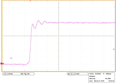 Figure 4 Switch Node Waveform for the QFN Package
FCOL QFN (TI Brands This Package as HotRod)
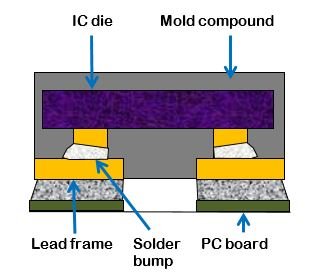 Figure 5 FCOL QFN Package Cross Section
The resulting performance, from the perspective of switch-node ringing, is measurably improved because there are no wires connecting the IC to the lead frame and PCB. The connection is much shorter and direct between the IC and outside world. Not surprisingly, when observing the switch-node waveform (under the same conditions as for TSSOP and QFN), there is a significant reduction (almost a complete absence) of switch-node ringing. Figure 6 shows switch-node ringing on the LM53635 device.
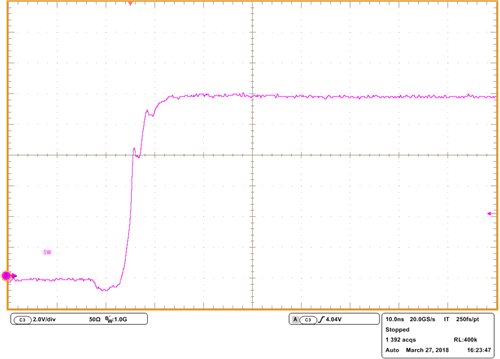 Figure 6 Switch Node Waveform for the FCOL QFN Package
Based on your desired performance and application constraints, you should carefully consider package type an important selection criteria. The new device generations show significantly improved performance in terms of switch-node ringing.
Understand, however, that switch-node ringing is just one of the performance parameters that will affect EMI performance in the end application. You will need to account for several other factors such as proper input filtering, board layout and the appropriate selection of passive components for optimum performance. Download the application report, “Designing High-Performance, Low-EMI Automotive Power Supplies.”