SSZT824 January 2018 LMZM23601
Certain applications, such as test and measurement, are sensitive to voltage ripple and routinely require very low output voltage ripple. For example, 10µV/V of ripple ratio translates to 100dB of attenuation.
Since it’s impractical to attain this level of attenuation using a buck regulator with a single-stage filter, a powerful design technique to reduce output voltage ripple is to use a second-stage inductor-capacitor (LC) filter, as shown in Figure 1. Proper configuration of the second-stage filter is essential for optimal performance.
 Figure 1 Buck with a Second-stage LC
Filter
Figure 1 Buck with a Second-stage LC
FilterIn order to obtain a total of 100dB attenuation at the switching frequency, the first and second LC filter are designed to give an attenuation A1 (60dB) and A2 (40dB), respectively. For the first-stage filter, inductor L1 is designed to give a chosen ripple ratio based on the load current. In power modules, this L1 inductor is integrated inside the package.
Equation 1 expresses the impedance of inductor L1 at the switching frequency as:
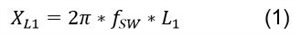
Therefore, Equation 2 expresses the impedance of C1 at the switching frequency as:
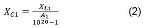
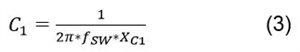
Equation 3 translates the required impedance XC1 to the value of capacitor C1:
The impedance of the filter should be sufficiently low at the output so that it does not significantly affect the loop gain of the converter. Low output impedance also helps with better regulation over long trace lengths. This is particularly true in systems where you can’t maintain the load that the regulator is driving in close proximity to the regulator. As we can see from Figure 2, the ratio of first-stage capacitance (C1) to second-stage capacitance (C2) is critical to the impedance of the converter.
To ensure low impedance and make sure that the filter doesn’t substantially affect the loop, I set the ratio of C1 to C2 as 1 to10.
 Figure 2 Closed Output Impedance with
Different Filter Designs
Figure 2 Closed Output Impedance with
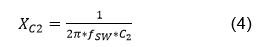
Different Filter DesignsEquation 4 expresses the impedance of C2 at the switching frequency:
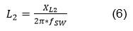
To get A2 attenuation, Equation 5 determines the impedance of L2 as:
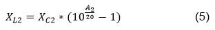
Equation 6 translates the required impedance XL1 to the value of capacitor L2:
Many designers worry that the additional poles and phase delay of a second-stage filter will compromise loop stability. Actually, if you locate the additional double pole far away from the crossover frequency and keep it lower than the switching frequency, it won’t affect the bandwidth and phase margin of the converter.
What you should pay more attention to is the Q of the second-stage filter. A high Q will lead to a low gain margin (as shown in Figure 3) and consequently unstable operation, such as an undamped response to a step input. So you must damp the Q of the second-stage filter, and there’s more than one way to do it.
The easiest approach is to use electrolytic or polymer capacitors with equivalent series resistance (ESR). ESR is not a dependable factor, however, and would result in a reduction of ripple attenuation (an increase in output ripple). Another option is to add a resistor in parallel with the filter inductor as shown in Figure 4, which has the advantage of small size and low cost. The drawback is that it reduces the effectiveness of the filter at high frequencies because it reduces the effective impedance of the filter inductor.
 Figure 3 A High Q Results in Low
Phase Margin
Figure 3 A High Q Results in Low
Phase Margin Figure 4 Placing the Resistor
Parallel to the Inductor Damps the Q
Figure 4 Placing the Resistor
Parallel to the Inductor Damps the QLet’s use the LMZM23601 as an example, with VIN = 24V, VOUT = 5V, FSW = 750kHz and IOUT = 1A. The power module has a 10µH integrated inductor. So the impedance of L1 at the switching frequency is 47.1Ω. To get 60dB of attenuation for the first-stage filter, the impedance of C1 at the switching frequency should be 47mΩ, which is 4.5µF translated to capacitance. I chose 6.8µF to add some margin. Since the second-stage capacitor is set to 10x the first stage, the chosen value for C2 can be 68µF. The resulting impedance XC2 at the switching frequency is 3.1mΩ.
To obtain the remaining 40dB of attenuation, the impedance XL2 should be 309mΩ, which is 65nH when translated to inductance. Since this inductor is going to see the output current, it is important to design for enough margin so that the inductor doesn’t derate with current. You could choose a 160nH inductor. In order to damp the Q, I added a 250m resistor parallel to inductor L2.
Figure 5 shows the parameters I used in my example.
 Figure 5 The LMZM23601 with a
Second-stage Filter
Figure 5 The LMZM23601 with a
Second-stage Filter Figure 6 Test Output Voltage
Ripple
Figure 6 Test Output Voltage
Ripple Figure 7 Bode Plot with and without
the Second-stage Filter
Figure 7 Bode Plot with and without
the Second-stage FilterAs you can see from Figure 6 and Figure 7, adding a second-stage filter is an effective way to reduce output voltage ripple. You can easily get 0.014% (0.7mV/5V) of output voltage ripple, which is good enough for most applications. At the same time, proper filter design won’t affect the stability of the converter. Learn more about TI DC/DC power modules.